

 0
0
 0
0
By Kelvin S. Yuk, George R. Branner, David J. McQuate
Originally appears: Transactions on Microwave and Theory and Techniques, Dec 2009
A complete empirical large-signal model for high-power AlGaN/GaN HEMTs (GaN HEMT) utilizing an improved drain current (Ids ) formulation with self-heating and charge-trapping modifications is presented. The new drain current equation accurately models the asymmetric bell-shaped transconductance (gm ) for high Ids over a large range of biases. A method of systematically employing dynamic IV behavior using pulsed-gate IV and pulsed-gate-pulsed-drain IV datasets over a wide variety of thermal and charge-trapping conditions is presented. The composite nonlinear model accurately predicts the dynamic IV behavior, S-parameters up to 10 GHz, and large-signal wideband harmonic behavior for a multitude of quiescent gate-source and drain-source biases as well as third-order intermodulation distortion (IM3).
I. Introduction
As the development of wide bandgap semiconductors continues to grow, AlGaN/GaN HEMTs (GaN HEMTs) are arising as a forefront in high power microwave electronics. Many desirable characteristics of GaN HEMTs such as high breakdown voltage, high frequency operation and high power density make it a leading technology for wideband, high-efficiency, high-power microwave circuits. Recently, GaN HEMT amplifiers producing as much as 800 W at S-band have been reported making the technology an increasingly viable option for high power, integrated microwave systems [1]. Many applications such as mixers, oscillators, and power amplifiers have been developed using GaN HEMT technology [2]–[5]. As these devices are pushed to their power limitations, new methods of utilizing nonlinearities have been produced. Recent work in power amplifiers utilizing the manipulation of harmonics to achieve increased efficiency, output power, and gain have been reported [4], [5]. This has led to the desire for nonlinear models which accurately predict harmonic generation at the gate reflected and drain output terminals. The accurate utilization and re-manipulation of these harmonics are the driving force in developing models which predict highly nonlinear operation.
As a relatively immature, high power density device technology GaN HEMTs can exhibit significant self-heating and trapping effects which introduce anomalies and performance degradations at RF. Among recently reported analytical, large-signal models for GaN HEMTs [6]–[15], a majority focus on characterizing drain–source current (Ids ) dispersion from self-heating using dissipated power computations [7]–[10] and charge-trapping effects using transient delay networks [7], [9]. Furthermore, advanced studies on the complex thermal behavior of GaN HEMTs have also been conducted and implemented in large-signal models with good results [11], [12]. However, few report Ids predictions valid beyond 1 A and only a handful report predictions of higher order harmonics [10], [13]. Using techniques presented in [14]–[16], we develop an improved Ids formulation for modeling the unique transconductance (gm ) characteristics of high power GaN HEMTs. Extensive use of dynamic IV measurements can be used to characterize the device performance and exploit thermal and trapping effects with great success [17], [18]. Accurate self-heating and charge-trapping models due to dissipated power and the applied quiescent biases are integrated into the Ids model in a complete modeling methodology. The resulting general-purpose nonlinear model accurately predicts pulsed Ids behavior up to 2.3 A at drain–source voltages up to 56 V, S-parameters up to 10 GHz and large-signal output (Pout ) and input reflected power (Prefl ) up to 39 dBm incident power for three harmonics. This work represents a significant expansion of [15] in terms of power, bias, large-signal frequency response and optimal load validity.
This paper presents an empirical large-signal model utilizing the Cree Inc. CGH40010F 10 W RF Power GaN HEMT [19]. The unmatched GaN HEMT is contained in a flange-type 440166 package and measures approximately 14.09 mm x 4.19 mm x 3.43 mm. Characterization of this device was performed with the device mounted on an aluminum test fixture secured to a heat sink and fan which permits efficient transfer of heat generated from the device under high power dissipation. The complete empirical circuit model is implemented using the Agilent Advanced Design System (ADS) software.
A complete description of the model is provided in Section II. First, the Ids formulation predicting the asymmetric bell-shaped gm and high current output is presented and applied to pulsed-gate IV (PGIV) characteristics [20]. Second, a thermal modification for predicting the effects of self-heating due to dissipated power is described. Third, a gate–source voltage modification which models charge-trapping effects is presented. The validity of the dynamic IV model is demonstrated through comparisons with PGIV and pulsed-gate-pulsed-drain IV (PIV) [21], [22] characteristics under various quiescent gate-source (Vgsq ) and quiescent drain-source (Vdsq) biases. In Section III, the complete large-signal model is validated using small-signal S-parameters and large-signal input reflected and output power measurements over various incident RF levels, biases and frequencies. Predictions of high power third-order intermodulation distortion products (IM3) are also presented. Large-signal predictions of the device terminated under optimal load conditions for maximum Pout are also presented. Section IV summarizes and concludes this work.
II. Model Description
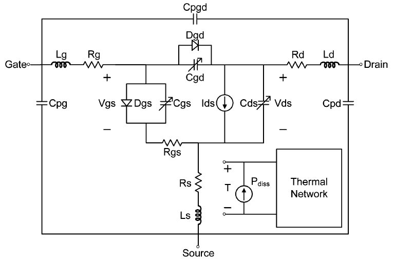
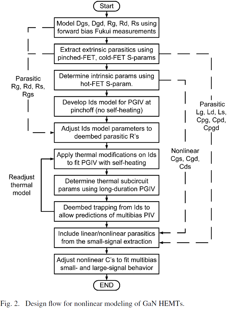
The complete nonlinear model is shown in Fig. 1. The nonlinear elements of the model consist of the drain source current (Ids), bias dependent capacitances Cgs, Cds, Cgd, and diodes Dgs and Dgd. The linear elements are the package resistances, inductances and capacitances. The thermal subcircuit which computes the transient self-heating behavior is also identified in Fig. 1. The complete design flow for the development of the nonlinear model is shown in Fig. 2. The process illustrates the extraction of parasitics from S-parameter measurements, followed by the application of the Ids equation, integration of thermal and charge-trapping modifications and finally the assembly of the constituting elements to form the complete model.
The description of the Ids model will be given first (see Section II-A) along with its employment on PGIV characteristics (see Section II-B). Following this, the development of the self-heating model (see Section II-C) and charge trapping model (see Section II-D) will be presented. Then, the parasitic element extraction (see Section II-E) and nonlinear diode modeling (see Section II-F) will be explained.
A. Modeling of High Power GaN HEMT Drain Current Characteristics
The Angelov model [23], [24] has frequently been used to model HEMT Ids due to improved predictions of device gm [7], [8]. An analytical drain–source current model based on [14], [15] is developed here for the high-power GaN HEMT. This new model is given by (1) as
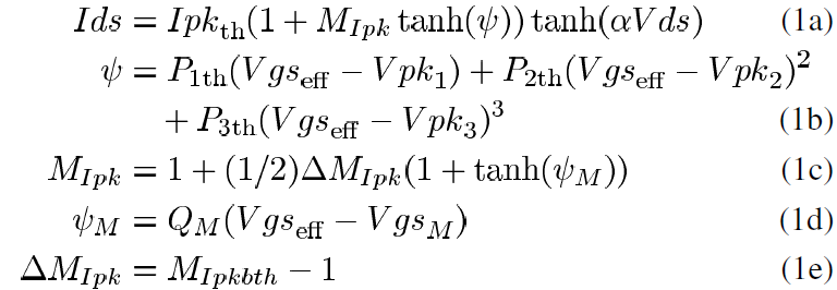
where Pn are the coefficients of the psi polynomial, MIpk is the hyperbolic tangent-based multiplier for Ipk, psiM, controls the shape of MIpk as a function of Vgs centered around VgsM, QM is the coefficient for psiM, and MIpkb defines the upper bound limit for MIpk.
In addition to its appearance in the tanh function in (1a), the drain–source voltage Vds appears in Pn, MIpkb and QM as shown in the following:
where Pn0, Pn1 alphaPn and Pno describe the Vds relationships for Pn; PM0, PM1, PM2, alphaM and PMo describe the Vds relationships for MIpkb; and PQ0, PQ1, alphaQ and PQo describe the Vds relationships for QM.
In contrast with the SiC MESFET device model presented in [16], the Ids formulation presented here accurately represents the highly asymmetric bell-shaped gm of the high power GaN HEMT. Since the gm of SiC MESFET devices does not peak, a model of increased complexity is required for high power GaN HEMT devices which exhibit a distinct peaking behavior. The measured and modeled gm versus Vgs at high Vds obtained from PGIV measurements is depicted in Fig. 3(a). The original Angelov model [23] which was not initially developed to model gm asymmetry is also shown in Fig. 3(a) for comparison. The corresponding Ids versus Vgs is shown in Fig. 3(b). Two modifications to the original Angelov model have been developed and implemented to permit accurate characterization of the characteristic gm shape for this class of device. The first modification assigns a unique Vpkn to each polynomial term of Psi in (1b). This creates the skewing of the bell-shaped gm [14], [15]. The second modification introduces a multiplier term MIpk in (1a) which allows the elongation of the gm bell-shape for Vgs>Vpk [15].
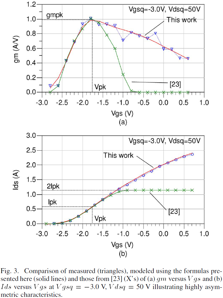
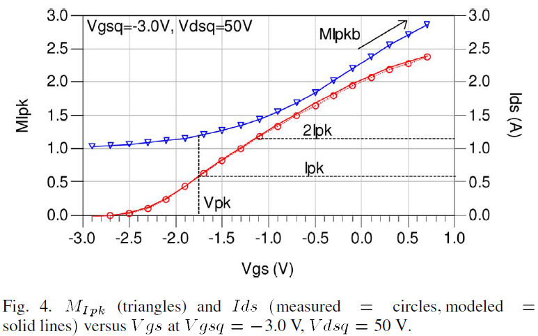
In early implementations of the Angelov model, MIpk=1 and the maximum drain current is equal to 2Ipk [23]. However, examination of the measured Ids behavior as a function of Vgs reveals that Ids increases to values well beyond the 2Ipk limit as shown in Fig. 3(b). The inclusion of MIpk permits the drain current to increase beyond 2Ipk as a function of Vgs and results in significantly improved accuracy. The MIpk function is shown in Fig. 4. For Vgs<Vpk, MIpk stays close to a value of 1.0 but for Vgs>Vpk, MIpk increases and, in turn, elongates the Ids characteristic. As a consequence, an accurate portrayal of the slow decline of gm from its peak value is developed.
The drain–source voltage relationships for parameters Pn, MIpkb and QM shown in (2a), (2b), and (2c), respectively, permit modeling of Ids and gm across Vds values. Those Vds relationships share a similar form and are necessary in modeling the subtle complexities of the knee region illustrated in Section II-B.
B. Application of the Drain Current Model on PGIV Characteristics
Employing the new Ids formulation described above on an IV dataset free of self-heating and charge trapping would be the ideal approach. However due to power limitations in available PIV systems, it is difficult to obtain high power PIV data. In this work, those are circumvented by characterizing Ids based on high power PGIV and then de-embedding the effects of charge-trapping using lower power multi-bias PIV measurements [15], [16].
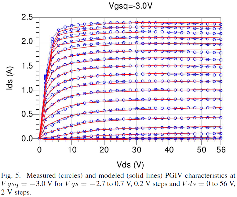
In order to acquire adequate data for model development, multiple PGIV datasets were taken to obtain the device’s performance under controlled static self-heating and trapping conditions. The new Ids formulation of (1) and (2) is first employed to model the PGIV device characteristics with a quiescent gate bias below pinchoff at the value Vgsq_pinch=-3.0 V. Below pinchoff, the device dissipates no power and consequently, is free of any static self-heating conditions. The device’s response when held under this state will serve as a basis for modeling Ids. The outcome of the application of the new Ids model is illustrated in Fig. 5 for Vgsq_pinch=-3.0 V. These results are presented for Vgs ranging from -2.7 to +0.7 in 0.2 V steps with drain voltages ranging from 0 to 58 V. Pulse durations of 100 ns were used since these are short enough to prevent the onset of dynamic self-heating and charge-trapping effects [22].
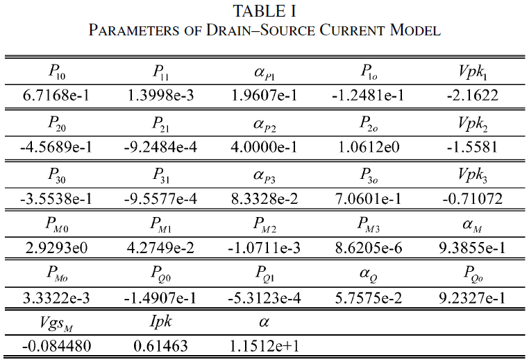
The curves of Fig. 5 show the high degree of precision resulting from using the new Ids formulation over a very large range of drain–source currents and voltages. Accurate characterization and modeling of pulse powers of up to 132 W at Vdsq=56V is observed. The resulting Ids model parameters are provided in Table I.
C. Modeling of Dispersive Phenomena Due to Self-Heating
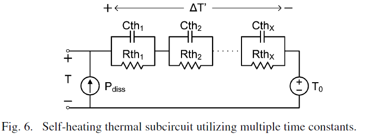
The self-heating thermal subcircuit utilizing multiple time constants shown in Fig. 6 serves as an electrical analog in modeling the thermal charging and discharging behavior of the device. The thermal model presented here is a generalization of the single time constant models presented in [7], [15], [16], [24]. This multiple time constant model is highly accurate in computing the transient temperature behavior as a function of dissipated power as described by the expression
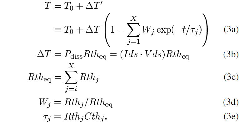
In (3), T0 is the ambient temperature, deltaT’ is the time-varying temperature change, Pdiss is the instantaneous dissipated power and Rth_eq is the equivalent thermal resistance. The thermal time constants tau_j are determined by the product of the thermal resistance and capacitance pairs, Rth_j and Cth_j, respectively, and X is the number of time constants. The coefficients Wj are determined by the ratio of Rth_j to Rth_eq. A constant Rth_eq value of 5.0 C/W is used in the model [19].
In modeling the thermal effects on the Ids response, it is first necessary to identify the temperature-sensitive parameters of the model. This is done by applying the generalized Ids formulation of (1), (2) to each individual available PGIV dataset to produce a unique set of parameters corresponding to each PGIV dataset. By comparing Ids parameters extracted from PGIV with self-heating with those extracted from PGIV at Vgsq_pinch with no self-heating, the temperature-sensitive parameters are identified as Ipk, P1, P2, P3 in (1a), (1b), and MIpkb in (1e). These parameters are represented as a function of the temperature change and drain–source voltage, respectively, by the following relations:
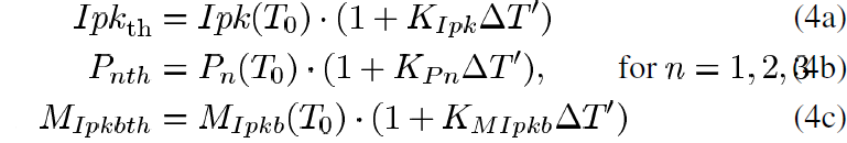
where Ipk(T0), Pn(T0) and MIpkb(T0) are computed with no self-heating and the bias-dependent thermal coefficients K_Ipk, K_Pn and K_MIpkb are given by
where K_Ipk0, K_Ipk1, K_Pn0, K_Pn1, K_MIpkb0, K_MIpkb1, alpha_KIpk, alpha_KPn, and alpha_KMIpkb are drain-source voltage fitting parameters [15]. The thermal relationships of (5) depend only on Vds and are simpler than those presented in [16] due to the use of a constant equivalent thermal resistance. Despite this simplification, the resulting formulations are adequate for use in predicting the pulsed electrical behavior of the device.
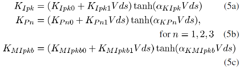
Determination of the multiple time constant parameters Rthj and Cthj is performed using long-duration PGIV measurements. A long-duration PGIV waveform with a 5 ms width and 500ms period is shown in Fig. 7 with Vds=28 V. At t=2ms, the gate is pulsed from Vgsq=-2.64V to Vgs=-1.7V and the subsequent Ids is excited from zero to a peak value of 600 mA. This is followed by a slow decay of Ids as thermal charging due to the dissipated power sets in. At t=7 ms, Vgs returns to -2.64 V and Ids falls back down to zero. Comparisons of Ids computed from the model using single and three time constants are also provided in Fig. 7. The simulations reveal that a single time constant model can only provide accuracy up to 0.2 ms and, as such, prematurely predicts the degradation of Ids to its quiescent value. In comparison, Fig. 7 shows that a three time constant model can provide accuracy over the entire 5 ms pulse duration. Since Rth_eq is a constant, it is important to note that the Rth_j values are related by (3c) to preserve the correct Ids-to-temperature relationships.
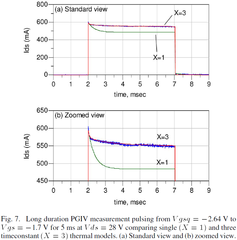
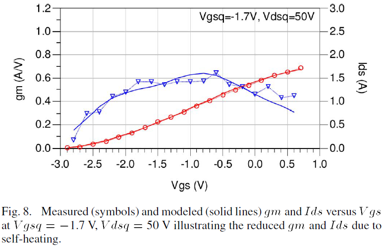
The efficacy of the above thermal modeling process is illustrated in the gm and Ids plots versus Vgs shown in Fig. 8. A perusal of the comparative measured data and modeled computations graphically illustrates the accuracy of the model for prediction of the reduced gm and Ids due to self heating. The thermally-modified drain–source relationships developed in (4) and (5) are demonstrated in Fig. 9 for a complete set of PGIV characteristics at Vgs=-1.7V. The close predictions validate the capability of the Ids formulation to accurately depict the reductions in drain current due to increased temperature at high dissipated power levels.
D. Modeling of Dispersive Phenomena Due to Charge-Trapping
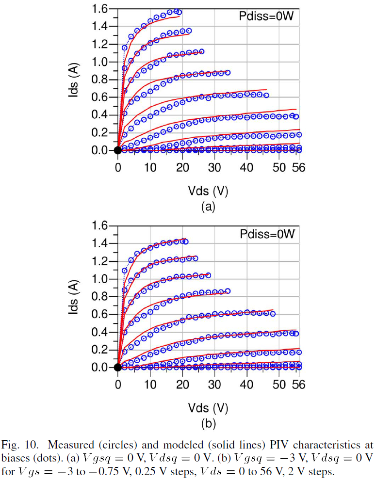
Although high power PGIV characteristics are applicable to characterize current dispersion, such measurements cannot differentiate the effects of self-heating from those of charge-trapping. In addition, they may not provide accurate predictions of output conductance (gds) at RF. Therefore, it is necessary for the Ids model to accommodate computations of both PGIV and PIV characteristics which will provide a better prediction of large-signal RF behavior for a given operating point. Charge-trapping effects in the GaN HEMT are observable by comparing the PIV characteristics at different quiescent points [25], [26]. A Nanometrics DiVA Dynamic I-V Analyzer [27] was used to measure the PIV characteristics of the GaN HEMT device for eight different quiescent biases employing 200ns pulse durations as shown in Figs. 10 and 11. Dynamic chargetrapping effects are avoided by using short duration pulses such that the differences between each PIV set are attributed to the static thermal and trapping effects associated with the quiescent bias only [22]. Since surface traps directly reduce the effect of the applied gate bias while substrate traps produce a backgate voltage, both effects can be modeled as a modification of the effective Vgs (Vgs_eff) [15], [16], [25], [26], [28].
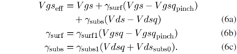
The Ids expression in (1) and (2) was applied to PGIV data and consequently includes static surface trapping effects dictated by Vgsq and static substrate trapping effects dictated by Vdsq. These effects can be de-embedded from the PGIV-based Ids expression by applying a model which determines Vgs_eff based on the degree of surface and substrate trapping exhibited at a particular quiescent bias. For applications with the current GaN model, the effective Vgs is presented in (6) as
The coefficient gamma_surf1 (Volts-1) and Vds_subs0 determines the influence of surface trapping based on the instantaneous Vgs and Vgsq relative to Vgsq_pinch. The coefficient gamma_subs(Volts-1) and Vds_subs0 determine the influence of substrate trapping as a function of the instantaneous Vds and Vdsq. In the case of the SiC MESFET [16], only a substrate trapping term was used. Here, the addition of the surface trapping term in (6a) and (6b) is necessary due to the GaN HEMT’s increased channel sensitivity to small variations in the gate potential resulting from surface traps. The device experiences less surface trapping as Vgsq increases above Vgsq_pinch. De-embedding of this effect from the Ids formulation is manifested as an increase in Vgs_eff in (6b). The influence of this increase is further enhanced at instantaneous Vgs pulsed above Vgsq_pinch shown in (6a). Similarly, the device experiences increased substrate trapping at higher Vdsq. When the instantaneous Vds is pulsed to values below a given Vdsq, Vgs_eff is reduced during that pulse due to backgating since the substrate trapping is dictated by the higher Vdsq. On the other hand, Vgs_eff is enhanced when the instantaneous Vds is pulsed above Vdsq. The substrate trapping relationships shown in (6a) and (6c) accurately account for this effect which is more pronounced as Vdsq increases.
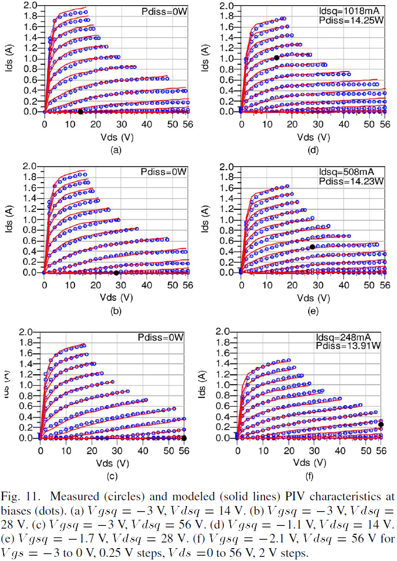
The accuracy of the surface trapping formulation is illustrated by comparing PIV characteristics biased in the absence of self-heating at the same quiescent Vdsq=0 V, but at different Vgsq. Inspection of the PIV characteristics biased at Vgsq=0 V, Vdsq=0 V [see Fig. 10(a)] and at Vgsq=-3 V, Vdsq=0 V [see Fig. 10(b)] show that the surface trapping model in (6a) and (6b) is valid over a large range of Vgsq. Similarly, the efficacy of the substrate trapping modification is illustrated by comparing PIV characteristics biased in the absence of self-heating at Vgsq_pinch, but at different Vdsq. Inspection of the PIV characteristics at Vgsq=-3.0 V, Vdsq=0 V [see Fig. 10(b)], at Vgsq=-3.0 V, Vdsq=14 V [see Fig. 11(a)] at Vgsq=-3.0 V, Vdsq=28 V [see Fig. 11(b)] and at Vgsq=-3.0 V, Vdsq=56 V [see Fig. 11(c)] show the expansive region of validity using the straightforward substrate trapping model in (6a) and (6c).
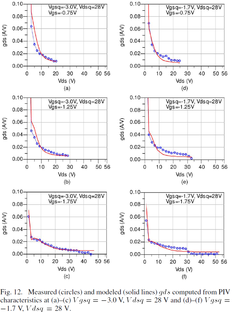
The accurate simultaneous operation of surface trapping, substrate trapping and self-heating models is graphically demonstrated by an examination of the PIV characteristics illustrated in Figs. 11(d)–(f). These data are for the Vgsq/Vdsq pair values of 1.1/14 V, 1.7/28V and 2.1/56V, respectively. Note that the power dissipated and therefore the temperature of the device under these three quiescent conditions are approximately the same. By comparing the PIV characteristics at -3.0 V, Vdsq=14 V [see Fig. 11(a)] and at Vgsq=-1.1 V, Vdsq=14 V [see Fig. 11(d)], the effects of surface trapping and self-heating can be observed at Vdsq=14 V. Likewise, by comparing the PIV characteristics at Vgsq=-3.0 V, Vdsq=28 V [see Fig. 11(b)] and at Vgsq=-1.7 V, Vdsq=28 V [see Fig. 11(e)], the effects of surface trapping and self-heating can be observed at Vdsq=28 V. Finally, by comparing the PIV characteristics at Vgsq=-3.0 V, Vdsq=56 V [see Fig. 11(c)] and at Vgsq=-2.1 V, Vdsq=56 V [see Fig. 11(f)] the effects of surface trapping and self-heating can be observed at Vdsq=56 V. Select output conductances of PIV characteristics at Vdsq=28 V are also shown in Fig. 12.
One important conclusion is that surface trapping due to Vgsq above pinchoff cannot be distinguished from self-heating at Vdsq > 0 V. The thermal self-heating parameters are determined by biasing the device in a power-dissipative state at Vgsq = -1.7 V and comparing those PGIV characteristics with ones measured at Vgsq = -3.0 V. However, any nonzero Vgsq also causes surface trapping and the resulting difference between measured PGIV characteristics shown in Figs. 5 and 9 cannot be attributed solely to self-heating. The device exhibits less charge-trapping at Vgsq=-1.7 V than at Vgsq=-3.0 V but the performance degradation due to self-heating at Vgsq=-1.7 V is much more pronounced. As a consequence, after the gate–source trapping model is established using PIV measurements at Vdsq=0 V, the PGIV performance of the model at Vgsq=-1.7 V will overpredict Ids. Therefore, compensation can be performed by incrementally increasing the magnitude of the self-heating K parameters in (5) using optimization as described in the flow diagram of Fig. 2. The modeled results presented here in Figs. 3–12 represent the final, compensated Ids model.
E. Small-Signal Extrinsic and Intrinsic Parasitic Extraction and Modeling
The extrinsic and intrinsic parasitic parameters of the device were extracted using S-parameters measured on an Agilent E8364B PNA from 0.2 to 10.0 GHz over a wide variety of quiescent biases using well-developed methods [29], [30]. The extrinsic capacitances were extracted from pinched-FET S-parameters, while the extrinsic inductances and resistances were extracted using cold-FET S-parameters. Numerous hot-FET S-parameter datasets were used to extract the intrinsic bias-dependent capacitances. These nonlinear capacitances Cgs, Cgd, and Cds were implemented using the charge-equation-based nonlinear capacitance models in [24].
F. Nonlinear Gate–Source and Gate–Drain Diodes
The nonlinear gate–source and gate-drain diode characteristics were measured using forward bias IV measurements and modeled using the Shockley ideal diode equation. The forward conduction characteristics of the device were also employed to assist the extraction of the parasitic terminal resistances as described by [31].
III. Experimental Model Verification Under RF Drive
The RF performance of the model compared with measured data is presented in the discussion below. To demonstrate the efficacy of the modeling process detailed in this work, smallsignal RF comparisons followed by single-tone and wideband large-signal RF comparisons will be made for two representative biases: Vgsq=-2.5 V, Vdsq=28 V and Vgsq=-1.9 V, Vdsq=28 V. Model predictions of IM3 will be also be illustrated. Finally, the model will be verified at large-signal under an optimum load which provides maximum fo output power.
A. Small-Signal S-Parameters
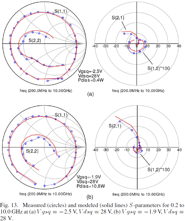
S-parameter simulations of the GaN HEMT model for the two representative biases were performed over a frequency range of 0.2 to 10 GHz and show close agreement with measured data (see Fig. 13). Since the two representative biases exhibit different power levels and quiescent terminal voltages, proper representations of the device at RF require correctly derived self-heating and trapping models. Validation of the model for small-signal operation suggests that the PGIV- and PIV-based drain current implementation provides accurate prediction of gm and gds at RF frequencies and under various self-heating and charge-trapping conditions. Furthermore, correct extraction and modeling of the parasitic extrinsic and intrinsic elements are also validated.
B. Large-Signal Harmonics Versus Incident Power
Under large signal drive conditions, Ids and Vds exhibit clipping behavior which results in output power saturation and the generation of harmonics. Simultaneously, the unmatched gate terminal generates significant reflected harmonic power due to device nonlinearities. Therefore, it is important for a general nonlinear model to accurately predict both output and input reflected harmonics. Additionally, for applications such as high efficiency power amplifiers, computations of reflected power can aid in improving power added efficiency (PAE).
The model was assessed under large signal excitations over an available source power (Pavs) ranging from 10 to 39dBmat fo=3.333 GHz in a 50 ohm system. The input reflected (Prefl) and output generated (Pout) power were measured under these excitations for three harmonics and for the two representative biases as shown in Fig. 14, respectively. A comparison of these measured and modeled results demonstrates the model’s capability to accurately predict the large-signal behavior.
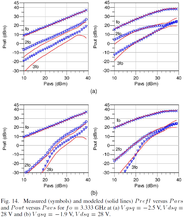
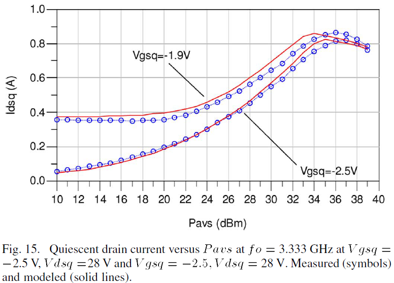
A perusal of the harmonic data at these two quiescent biases provides an assessment of harmonic generation as a function of Pavs. Starting at low Pavs, the harmonic generation at the input and output differ greatly between the two biases. At Vgsq=-2.5 V [see Fig. 14(a)], there is generally more 2fo and 3fo generation at both ports while for Vgsq=-1.9 V [see Fig. 14(b)], there is generally more fo output power. Beyond Pavs=+33 dBm the device output saturates and the generated Pout and Prefl harmonic power levels are about the same for both biases. At these high power levels, the quiescent operating points converge to the same value regardless of the applied DC bias due to the shift in Idsq that occurs under large signal RF drive as shown in Fig. 15. Fig. 15 illustrates that Idsq increases until Pavs=+36 dBm at which time Dgs is pushed in forward conduction and the resulting Idsq saturates. The capability to track this Ids behavior is assisted by the accurate self-heating model which continuously adapts the device output characteristics based on increasing static power dissipation and to the correctly implemented hard clipping mechanisms of the gate-source diode.
C. Broadband Large-Signal Harmonic Power
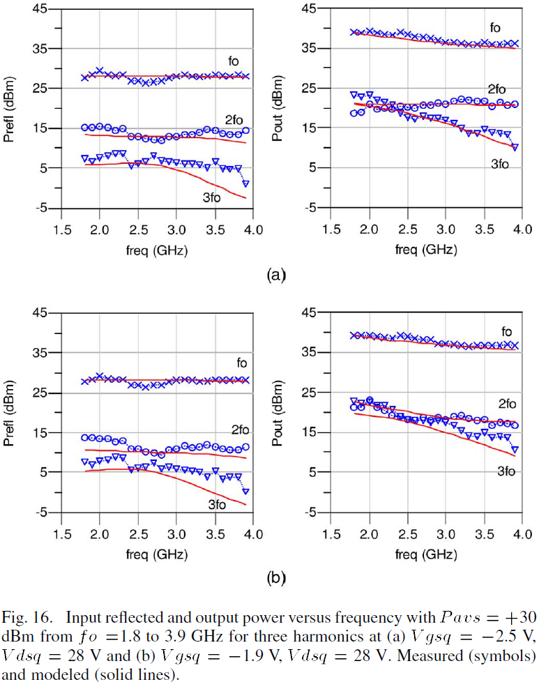
One of the main advantages of GaN HEMTs is their ability to operate over wide frequency ranges. The broadband large-signal performance of the model has been examined over a frequency range from 1.8 to 3.9 GHz which corresponds to 73% fractional bandwidth centered at fo=2.85 GHz. This is over an octave of bandwidth and covers a majority of the S-band. The large-signal wideband harmonic predictions at the input reflected and output ports using the model presented here are compared with measured data in Fig. 16(a) and (b) for the two representative biases, respectively. The wide frequency coverage of the model highlights its use as a high-precision, broadband nonlinear model.
D. Third-Order Intermodulation Distortion (IM3)
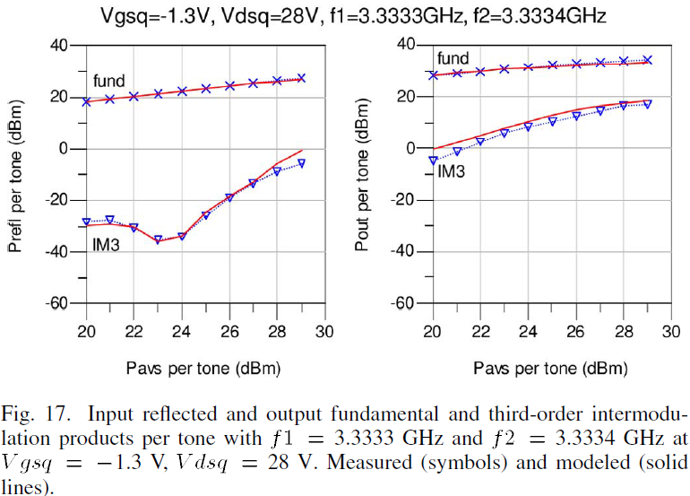
The third-order intermodulation distortion products at the input reflected and output ports has been measured using a two-tone test conducted with f1=3.3333 GHz and f2=3.3334 GHz for a 100 kHz tone spacing over an available source power of 20 to 29 dBm per tone with device biasing at Vgsq=-1.3 V, Vdsq=28 V. Since this is an unmatched device, significant IM3 products will be generated due to nonlinear input reflection at the gate in addition to nonlinear output at the drain. According to swept IM3 characteristics shown in Fig. 17, the large-signal model closely matches the distortion behavior over the high two-tone power levels, allowing the model to predict device linearity.
E. Large Signal Output Under Optimal Fundamental Load
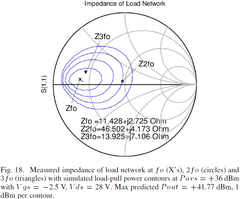
In order to verify the large-signal accuracy of the device model under a different load termination, the impedance at fo=3.333 GHz delivering maximum fundamental output power was determined for Pavs=+36 dBm using load-pull simulations of the model biased at Vgsq=-2.5 V, Vdsq=28 V. This optimal impedance at fo was realized using a distributed binomial impedance transformer. The values of the realized impedances at fo (Zfo), fo (Z2fo), and 3fo (Z3fo) of this network are shown in Fig. 18 along with the simulated load-pull power contours produced in ADS.
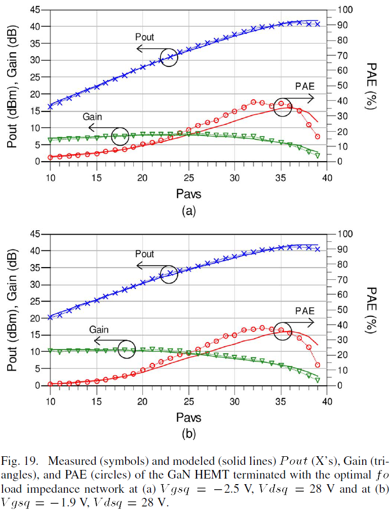
The measured and modeled large signal output power sweep of the device terminated in the realized network is shown in Fig. 19 for both representative biases over Pavs=+10 to +39 dBm. At Pavs=+37 dBm, the peak fundamental RF output power produced by the device is 41.17 dBm (13.09 W) for Vgsq=-2.5 V and +41.06 dBm (12.78 W) for Vgsq=-1.9 V and is predicted closely by the model. The gain and PAE are also provided in Fig. 19(a) and (b). These results show that the model can predict the very high output power levels under an optimum fo load impedance with good accuracy.
IV. Conclusion
A complete empirical large-signal model with a self-heating thermal subcircuit for high-power GaN HEMTs is presented in this paper. A newly developed large-signal drain current equation has demonstrated the capacity to efficiently model self-heating and charge-trapping effects through accurate predictions of high-power PGIV and PIV characteristics. The complete model with package parasitics, nonlinear capacitances and nonlinear diodes has demonstrated the ability to accurately predict the behavior of the device under small-signal RF operation over a wide bandwidth, large-signal RF operation for three harmonics at multiple biases and over a wide band of frequencies. The model has also demonstrated the capability to predict third-order intermodulation distortion products. Furthermore, the model can accurately predict large-signal output of the device under load conditions optimized for maximum output power.
The complete nonlinear model presented here and its accurate predictions support its value in studying the behavior and manipulation of two-terminal harmonic generation in high-power microwave GaN HEMT circuits.
Acknowledgment
The authors would like to thank Dr. I. Angelov, Chalmers Institute of Technology, Göteborg, Sweden, for his helpful discussions; Dr. G. Anderson, Clear Stream Technologies, Fulton, CA, Dr. W. Martin, The Aerospace Corporation, El Segundo, CA, for their generous contributions and support of this work; and Ms. C. Wong, University of California, Davis for her technical assistance.
References
[1] E. Mitani, M. Aojima, and S. Sano, “A kW-class AlGaN/GaN HEMT pallet amplifier for ????-band high power application,” in Proc. Eur. Microw. Integr. Circuits Conf., Oct. 2007, pp. 176–179.
[2] M. Sudow, K. Andersson, M. Fagerlind, M. Thorsell, P.-A. Nilsson, and N. Rorsman, “A single-ended resistive -band AlGaN/GaN HEMT MMIC mixer,” IEEE Trans. Microw. Theory Tech., vol. 56, no.10, pp. 2201–2206, Oct. 2008.
[3] H. Xu, C. Sanabria, S. Heikman, S. Keller, U. K. Mishra, and R. A. York, “High power GaN oscillators using field-plated HEMT structure,” in IEEE MTT-S Int. Microw. Symp. Dig., Jun. 2005, pp. 1345–1348.
[4] H. Otsuka, K. Yamanaka, H. Noto, Y. Tsuyama, S. Chaki, A. Inoue, and M. Miyazaki, “Over 57% efficiency -band GaN HEMT high power amplifier with internal harmonic manipulation circuits,” in IEEE MTT-S Int. Microw. Symp. Dig., Jun. 2008, pp. 311–314.
[5] P. Colantonio, F. Giannini, R. Giofre, E. Limit, A. Serino, M. Peroni, R. Romanini, and C. Proietti, “A -band high-efficiency second-harmonic-tuned hybrid power amplifier in GaN technology,” IEEE. Trans. Microw. Theory Tech., vol. 54, no. 6, pp. 2713–2722, Jun. 2006.
[6] P. M. Cabral, J. C. Pedro, and N. B. Carvalho, “Nonlinear device model of microwave power GaN HEMTs for high power-amplifier design,” IEEE Trans. Microw. Theory Tech., vol. 52, no. 11, pp. 2585–2592, Nov. 2004.
[7] I. Angelov, V. Desmaris, K. Dynefors, P. A. Nilsson, N. Rorsman, and H. Zirath, “On the large-signal modeling of AlGaN/GaN HEMTs and SiC MESFETs,” in Proc. Gallium Arsenide Other Semicond. Appl. Symp., Oct. 3–4, 2005, pp. 309–312.
[8] G. Torregrosa, J. Grajal, M. Peroni, A. Serino, A. Nanni, and A. Cetronio, “Large-signal modeling of power GaN HEMTs including thermal effects,” in Eur. Microw. Integr. Circuits Conf., Oct. 2007, pp. 36–39.
[9] O. Jardel, F. De Groote, T. Reveyrand, J.-C. Jacquet, C. Charbonniaud, J.-P. Teyssier, D. Floriot, and R. Quere, “An electrothermal model for AlGaN/GaN power HEMTs including trapping effects to improve large-signal simulation results on high VSWR,” IEEE Trans. Microw. Theory Tech., vol. 55, no. 12, pp. 2660–2669, Dec. 2007.
[10] A. Jarndal and G. Kompa, “Large-signal model for AlGaN/GaN HEMTs accurately predicts trapping- and self-heating-induced dispersion and intermodulation distortion,” IEEE Trans. Electron Devices, vol. 54, no. 11, pp. 2830–2836, Nov. 2007.
[11] V. Camarchia, F. Cappelluti, M. Pirola, S. D. Guerrieri, and G. Ghione, “Self-consistent electrothermal modeling of class A, AB, and B power GaN HEMTs under modulated RF excitation,” IEEE Trans. Microw. Theory Tech., vol. 44, no. 9, pp. 1824–1831, Sep. 2007.
[12] F. Bonani, V. Camarchia, F. Cappelluti, S. Guerrieri, G. Ghione, and M. Pirola, “When self-consistency makes a difference,” IEEE Microw. Mag., vol. 9, no. 5, pp. 81–89, Oct. 2008.
[13] C. T. Rodenbeck and R. Follmann, “Accurate prediction of large-signal harmonic distortion in gallium nitride HEMTs,” Electron. Lett., vol. 43, no. 10, pp. 590–591, May 10, 2007.
[14] I. Angelov and D. Schreurs, “Empirical device models,” presented at the Workshop, Adv. Active Device Char. Model. for RF Microw. (IMS), Honolulu, HI, Jun. 4, 2007.
[15] K. S. Yuk, G. R. Branner, and D. J. McQuate, “An improved empirical large-signal model for high-power GaN HEMTs including self-heating and charge-trapping effects,” in Proc. IEEE MTT-S Int. Microw. Symp., Jun. 2009, pp. 753–756.
[16] K. S. Yuk and G. R. Branner, “An empirical large-signal model for SiC MESFETs with self-heating thermal model,” IEEE Trans. Microw. Theory Tech., vol. 56, no. 11, pp. 2671–2680, Nov. 2008.
[17] F. Filicori, G. Vannini, A. Santarelli, A. M. Sanchez, A. Tazon, and Y. Newport, “Empirical modeling of low-frequency dispersive effects due to traps and thermal phenomena in III-V FET’s,” IEEE Trans. Microw. Theory Tech., vol. 43, no. 12, pp. 2972–2981, Dec. 1995.
[18] T. Fernandez, Y. Newport, J. Zamanillo, A. Tazon, and A. Mediavilla, “Extracting a bias-dependent large signal MESFET model from pulsed I/V measurements,” IEEE Trans. Microw. Theory Tech., vol. 44, no. 3, pp. 372–378, Mar. 1996.
[19] Cree, Inc., Durham, NC, “CGH40010 10 W, RF Power GaN HEMT Datasheet Rev. 1.3,” Mar. 2007. [Online]. Available: http://www.cree.com/products/pdf/CGH40010.pdf
[20] M. Paggi, P. H. Williams, and J. M. Borrego, “Nonlinear GaAs MESFET modeling using pulsed gate measurements,” IEEE. Trans. Microw. Theory Tech., vol. 36, no. 12, pp. 1593–1957, Dec. 1988.
[21] T. M. Barton, C. M. Snowden, J. R. Richardson, and P. H. Ladbrooke, “Narrow pulse measurement of drain characteristics of GaAs MESFET’s,” Electron. Lett., vol. 23, pp. 686–687, 1987.
[22] P. Ladbrooke, “Pulsed IV measurement of semiconductor devices,” Accent Optical Technologies, Bend, OR, pp. 1-9–1-18.
[23] I. Angelov and H. Zirath, “New empirical nonlinear model for HEMT devices,” Electron. Lett., vol. 28, no. 2, pp. 140–142, Jan. 1992.
[24] I. Angelov, N. Rorsman, J. Stenarson, M. Garcia, and H. Zirath, “An empirical table-based FET model,” IEEE Trans. Microw. Theory Tech., vol. 47, no. 12, pp. 2350–2357, Dec. 1999.
[25] D. Siriex, D. Barataud, R. Sommet, O. Noblanc, Z. Ouarch, C. Brylinski, J. P. Teyssier, and R. Quere, “Characterization and modeling of nonlinear trapping effects in power SiC MESFETs,” in IEEE MTT-S Int. Microw. Symp. Dig., Jun. 2000, vol. 2, pp. 765–768.
[26] Z. Ouarch, J. M. Collantes, J. P. Teyssier, and R. Quere, “Measurement based nonlinear electrothermal modelling of GaAs FET with dynamical trapping effects,” in IEEE MTT-S Int. Microw. Symp. Dig., Jun. 1998, vol. 2, pp. 599–602.
[27] Nanometrics, Inc., Milipitas, CA, “DiVA [Dynamic I-V Analyzer],” 2008. [Online]. Available: http://www.nanometrics.co.kr/products/Diva.html
[28] K. Kunihiro and Y. Ohno, “A large-signal equivalent circuit model for substrate-induced drain-lag phenomena in HJFETs,” IEEE Trans. Electron Devices, vol. 43, no. 9, pp. 1336–1342, Sep. 1996.
[29] R. Anholt, Electrical and Thermal Characterization of MESFETs, HEMTs, and HBTs. Boston, MA: Artech, 1995, pp. 36–44.
[30] G. Dambrine, A. Cappy, F. Heliodore, and E. Playez, “A new method for determining the FET small-signal equivalent circuit,” IEEE Trans. Microw. Theory Tech., vol. 36, no. 7, pp. 1151–1159, Jul. 1988.
[31] H. Fukui, “Determinations of the basic parameters of a GaAs MESFET,” Bell Syst. Tech. J., vol. 58, no. 3, pp. 771–797, Mar. 1979.