

 0
0
 0
0
By Kelvin Yuk, G.R. Branner and Claudia Wong
Originally appears: 2010 International Microwave Symposium Digest
High power, high conversion gain microwave frequency doublers using wide bandgap semiconductor devices are developed. A method of determining the optimal harmonic terminations using accurate nonlinear computer models and load- and source-pull simulations is described. Synthesis of these impedances using matching and reflector networks have produced doublers with increased output power, conversion gain and very high suppression of the first and third harmonics. A SiC MESFET-based frequency doubler at fo=2.00GHz producing up to 10.00dB conversion gain and 6.31 Watts 2fo output power is presented. An AlGaN/GaN HEMT-based frequency doubler at fo=3.33GHz producing up to 14.80dB conversion gain and 4.14W 2fo output power is also presented. The second harmonic power measurements confirm the accurate predictions made by the nonlinear model.
I. Introduction
Frequency multipliers play an important role in signal source generation and frequency conversion in microwave communication systems. Typically, a passive frequency multiplier is employed to multiply a signal source to the nth harmonic, followed by an output power amplifier (PA) for delivery to subsequent stages. While a nonlinear device such as a varactor diode may provide multiplication, this two-stage approach assigns constraints to the PA which include high gain and output power operation at the nth harmonic. One aspect of the development of active, high power frequency multipliers with high conversion gain is motivated by the desire to combine the functionality of the passive multiplier with the output PA. Such high conversion gain, high power active frequency multipliers permit elimination or relaxation of the PA requirements, thereby simplifying and improving the efficiency of the overall system.
Advances in wide bandgap semiconductor technologies such as silicon-carbide (SiC) and aluminum-gallium-nitride/gallium-nitride (AlGaN/GaN or GaN) have created new possibilities in high power, microwave integrated circuits. The manipulation of higher order harmonics in such devices has demonstrated improvements in power amplifier performance [1]. However, little work has been done in harmonic tuning for frequency multiplication in SiC MESFET and GaN HEMT devices [2]. This is due in part to the scarce availability of accurate nonlinear models which account for the dispersive effects inherent in these technologies, leaving measurement-based design strategies as the only option [3].
Several recent papers on frequency doublers have reported high conversion gain and moderate power levels [2],[4]-[7]. However none report power levels in excess of 1W at 2fo. In this work, high power, high conversion gain frequency doublers based on SiC MESFET and GaN HEMT technology are developed using precision nonlinear active device models. To the authors’ knowledge, these are the first microwave frequency doublers utilizing these devices demonstrating the capability of producing >4W at 2fo. This appears, therefore, to be the highest microwave output power of any single transistor frequency multiplier to date.
An overview of frequency doubler performance parameters is given in Section II. The design strategy of the bias and load and source networks is described in Section III. Large-signal measured performance of the realized doublers are provided in Section IV. Lastly, Section V concludes this work.
II. Microwave Frequency Doubler and Device Overview
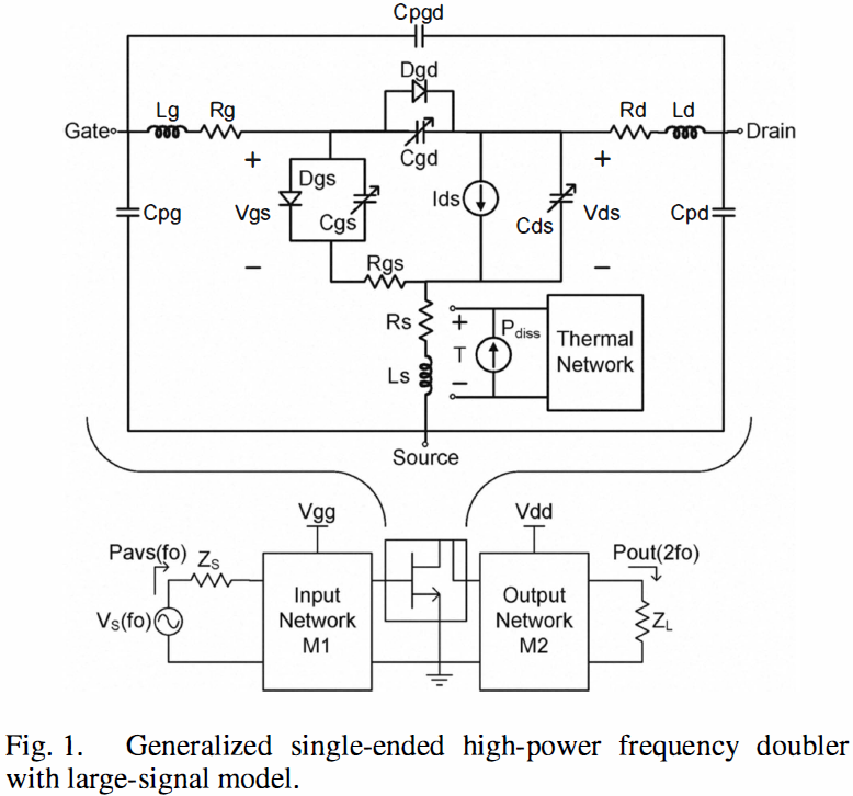
An unbalanced, single-transistor topology using harmonic reflection and matching networks is chosen for simplicity, low loss, cost and efficiency [8], [9]. Figure 1 illustrates a canonic realization of an ideal single-ended frequency doubler consisting of a high power active device coupled with performance-enhancing input and output networks.
The primary performance parameters under investigation for this frequency doubler are:
1. Output power at the second harmonic, Pout(2fo)
2. Conversion gain, CG(2fo)
3. Drain efficiency, η(2fo), and power added efficiency, PAE(2fo)
4. Suppression of unwanted fo and 3fo harmonics, Pout(fo)/Pout(2fo) and Pout(3fo)/Pout(2fo).
In this work, the commercially available devices employed to realize the doublers are the CRF24010 10W SiC MESFET [10] and the CGH40010F 10W GaN HEMT [11] devices, both manufactured by Cree, Inc. The high power density and relative immaturity of these wide bandgap devices result in substantial self-heating and charge-trapping effects. These dispersive effects can lead to poor predictions of harmonic generation if not properly taken into consideration. Fortunately, a substantial effort has been made to develop high-accuracy nonlinear models for both the SiC MESFET [12] and GaN HEMT devices [13] allowing for close performance predictions by the use of computerized design methods. The generalized circuit representation of the large-signal model for both devices is illustrated in Fig 1. The models and simulations presented here were performed employing the Agilent Advanced Design System (ADS) software package.
III. Design of High Power Frequency Doublers
The design of the SiC MESFET and GaN HEMT-based microwave frequency doublers is described in the ensuing paragraphs. Fundamental frequencies of 2.00GHz and 3.33GHz were employed for the SiC MESFET and GaN HEMT, respectively. The primary steps involved in the design are (a) selecting the appropriate device biasing, (b) determining the optimal source and load impedances which provide maximum Pout and CG, and (c) synthesizing these impedances into low-loss microstrip networks.
A. Device Biasing
Pinchoff bias is selected as the operating point of the SiC and GaN transistors for its numerous advantages. As shown in [14], pinchoff produces a half-wave rectified drain current waveform which is both rich in second and low in third harmonic content. Additionally, pinchoff produces no quiescent power dissipation, improving efficiency at low drive levels. Furthermore, the device has little gain at pinchoff resulting in stability under small-signal conditions. High drain-source voltage operation of the SiC and GaN devices allow for the increased generation of second harmonic power. A bias of Vgs=‑11V, Vds=55V for the SiC MESFET and Vgs=‑3.0V, Vds=28V for the GaN HEMT is selected.
In most practical cases, the predicted 2fo harmonic will quickly deviate from ideal once parasitic and frequency dependent elements are considered [8], [9]. Therefore, biasing alone will not lead to significant output power nor conversion gain and harmonic terminations aiding the generation and delivery of 2fo harmonic power are consequently essential.
B. Optimal Harmonic Load and Source Impedances
The optimal harmonic load and source impedances have been determined using harmonic load- and source-pull simulations in conjunction with highly accurate nonlinear device models [12], [13] implemented in ADS. A simplified schematic of the implementation for the case of two harmonics is shown in Fig. 2. This approach assumes no topology and is used as an analytical tool in investigating the effect of the harmonic impedances on device output. Due to the availability of the high-precision nonlinear models, harmonic load- and source-pull can be implemented in simulation and executed to provide extremely accurate, optimal results.
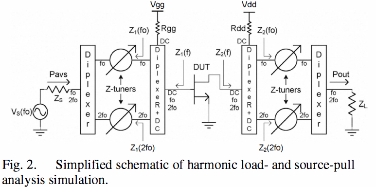
In Fig. 2, the ideal harmonic diplexer separates the signal path into two branches based on the specific frequencies at the input and output terminals of the device. Each branch is implemented with an impedance tuner to alter the port impedance at the particular harmonic of interest. In this procedure, the impedances Z1(fo), Z1(2fo) seen at the gate at fo and 2fo, respectively, and Z2(fo), Z2(2fo) seen at the drain are systematically swept about an a priori optimum in order to obtain the optimum output performance.
Although no assumption has been made about the network topology, harmonic reflector networks at both device ports can increase device performance through the constructive recycling of generated harmonics [8], [9]. A 2fo reflector placed at an optimal phase offset from the device input can improve conversion gain through linear 2fo amplification. Similarly, a fo reflector at an optimal phase offset from the device output can heavily suppress unwanted fo and 3fo output and improve both 2fo output power and gain through harmonic mixing at the drain.
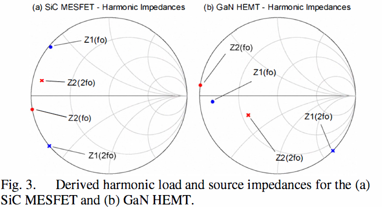
The determined harmonic impedances for the SiC MESFET and GaN HEMT designs are shown in Fig. 3.
C. Synthesis of the Load and Source Networks
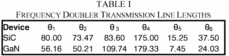
External bias tees are used for the frequency doubler prototypes and consequently attention will be focused on realizing Z1 and Z2 at RF. Straightforward, low-loss, narrowband microstrip stub networks are used to realize Z1 and Z2. The synthesized circuit topology is shown in Fig. 4. Each input and output network as viewed from the device ports consists of two stages: a harmonic reflector and a stub matching network. The synthesized offset phase lengths with respect to fo in degrees are tabulated in Table I for both the SiC MESFET and GaN HEMT designs.
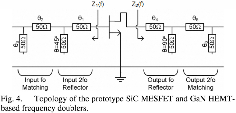
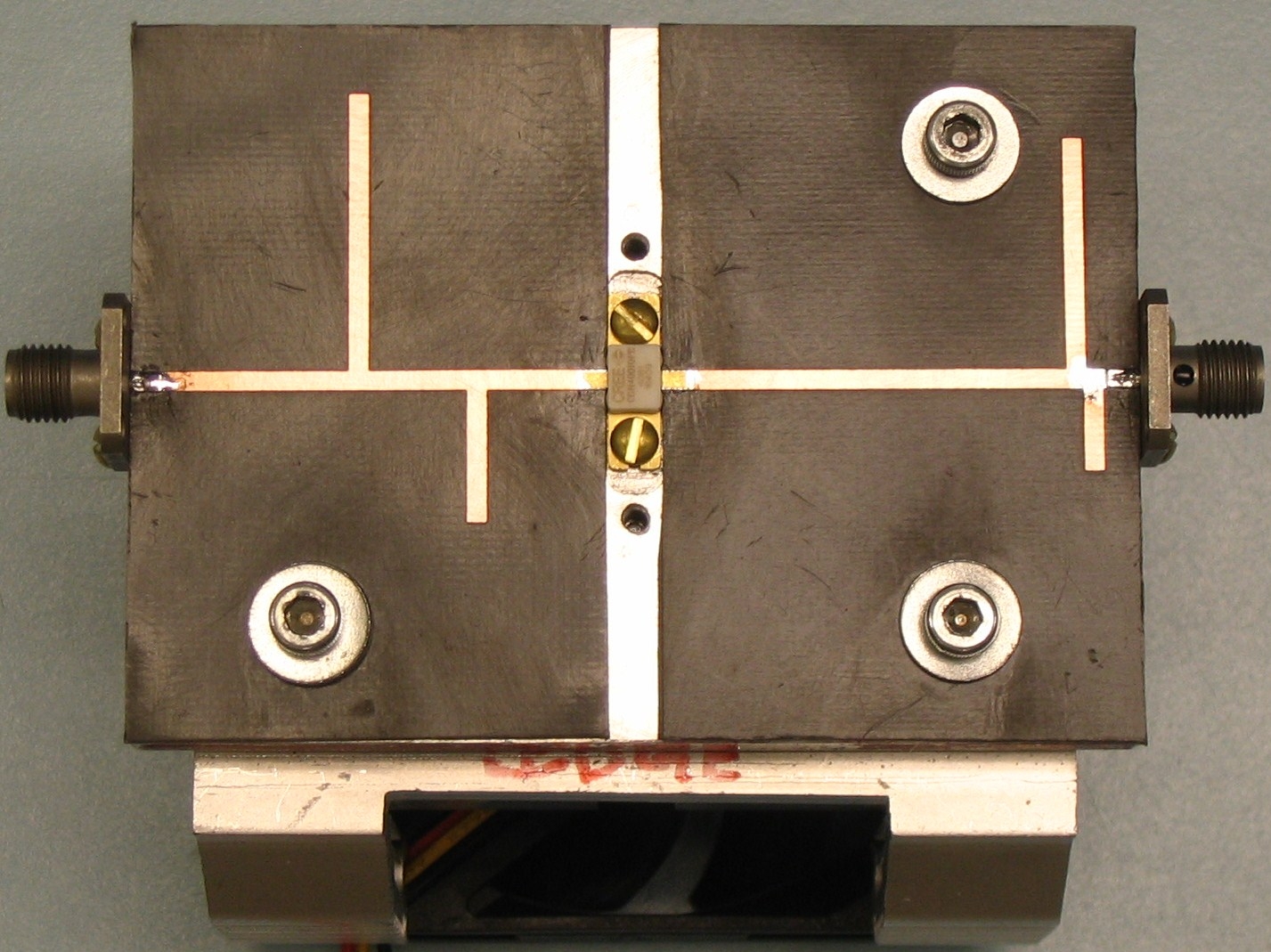
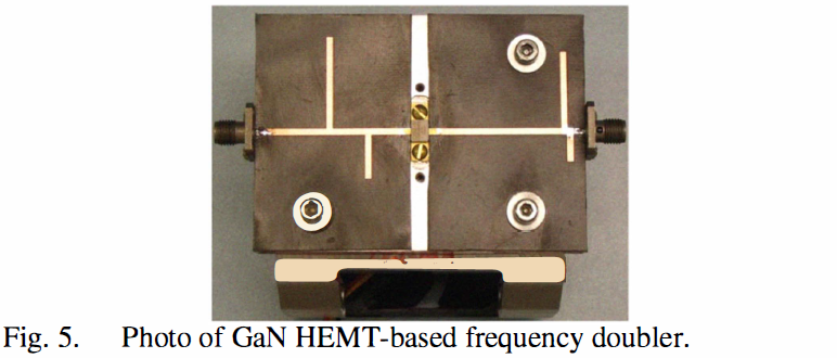
The networks were fabricated using Rogers RT/duroid 5880 microwave laminate. The reflector and matching network impedances are 50Ω which allow for safe reflection of the high power levels. The generation of excessive heat due to reflecting high power fo signal back into the drain of the device prevented the use of higher impedance lines having higher Q. The use of a 120Ω fo output reflector was attempted but resulted in a burned copper trace when subjected to high power operation. A photo of the GaN HEMT-based frequency doubler is shown in Fig. 5.
IV. Measurements and Circuit Performance
The performance of the SiC MESFET- and GaN HEMT-based doublers were measured under a wide range of large-signal drive conditions and compared with simulated results.
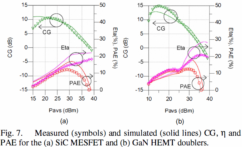
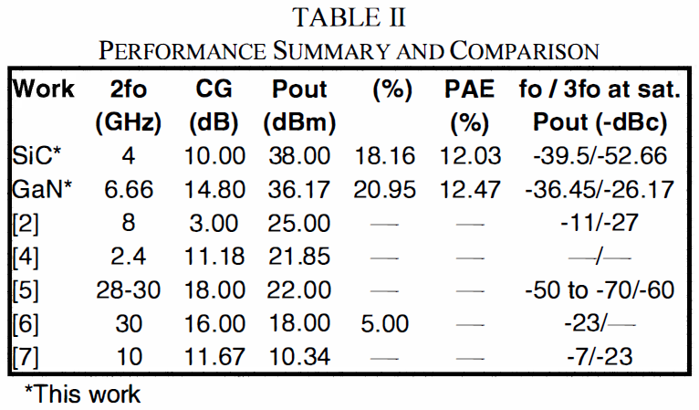
The large-signal harmonic output power of the SiC MESFET and GaN HEMT-based doublers are shown in Fig. 6a and 6b, respectively. Additionally, the CG, η and PAE for the 2fo output are shown for both designs in Fig. 7a and 7b, respectively. A perusal of these results reveals that a maximum Pout2fo of 38.00dBm (6.31W) has been achieved for the SiC MESFET doubler. Similarly, a maximum Pout2fo of 36.17dBm (4.14W) has been achieved for the GaN HEMT doubler. Also, an examination of these curves determines that a good suppression of the fo as well as the 3fo output power is achieved. These measurements show good agreement with the simulations. Table II compares the doublers’ maximum performance with that of recently published work.
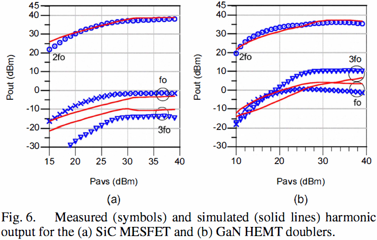
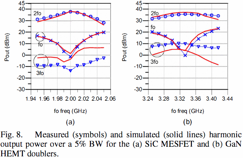
The output powers of the SiC MESFET and GaN HEMT doublers were assessed over a 5% fractional bandwidth around fo and the characteristics are provided in Fig. 8a and 8b, respectively. The SiC MESFET doubler is measured at an available power of +36dBm while the GaN HEMT doubler is measured at an available power of +33dBm. Simulations of the high power doublers are extremely close for the first and second harmonics. For the SiC MESFET doubler, the third harmonic falls 51.49dB below the second at the center frequency and consequently is more difficult to predict over a frequency range of interest. The 3dB bandwidths of the SiC MESFET and GaN HEMT doublers are 4.2% and 4.0%, respectively, due to the narrowband nature of the realized networks.
V. Conclusion
High power, high conversion gain frequency doublers employing silicon-carbide MESFET and gallium nitride HEMT devices have been developed using harmonic load- and source-pull simulations performed utilizing precision nonlinear device models. These models have been shown to closely predict the performance of the measured realized doublers. The performance demonstrated by this work appears to provide the highest frequency doubled output power reported for single-ended active frequency doublers.
Acknowledgement
The authors wish to acknowledge Dr. Wayne Martin and Dr. Giovonnae Anderson for their support and Swapnil Jain for his technical assistance.
References
[1] Y.-S. Lee, Y.-H. Jeong, “Applications of GaN HEMTs and SiC MESFETs in High Efficiency Class-E Power Amplifier Design for WCDMA Applications,” in IEEE MTT-S Int. Microw. Symp. Dig., pp. 1099 – 1102, Jun. 2007
[2] Y. Chung, K. M. K. H. Leong, and T. Itoh, “AlGaN/GaN HEMT X-band frequency doublers with novel fundamental frequency reflector scheme,” IEICE Trans. Electron., vol. E86-C, no. 8, pp. 1416-1421, 2003.
[3] R. Larose, F.M. Ghannouchi, R.B. Bosisio, “Multi-Harmonic Load-Pull: A Method for Designing MESFET Frequency Multipliers,” IEEE Military Communications Conference 1990, Conference Record, ‘A New Era’., vol. 1, pp. 466-469, 1990.
[4] D. Barataud, C. Arnaud, B. Thibaud, et. al., “Measurements of Time-Domain Voltage/Current waveforms at RF and Microwave Frequencies Based on the Use of a Vector Network Analyzer for the Characterization of Nonlinear Devices—Application to High-Efficiency Power Amplifiers and Frequency-Multipliers Optimization,” IEEE Trans. Instr. and Meas., vol. 47, no. 5, pp. 1259-1264, October 1998.
[5] S.-M. Nam, F. Traut, and J. Cuggino, “A Ka-Band High Power Frequency Doubler in SMT Package,” IEEE Compound Semicond. Integrated Circuit Symp.,”, pp. 61-64, Nov. 2006.
[6] S. Mahon, P. Beasly, J. Harvey, A. Bessemoulin, “A Broadband Millimetre-wave Differential pHEMT Frequency Doubler MMIC,” IEEE Compound Semicond.uctor Integrated Circuit Symp., pp. 212-215, Oct. 2005.
[7] Y. Chung, D. Ahn, and T. Itoh, “Alternating Input Power Dividing Technique for High Conversion Gain Frequency Doubler,” Euro. Microw. Conf., vol. 2, pp. 491-493, Oct. 2003.
[8] D.G. Thomas, Jr., and G.R. Branner, “Single-Ended HEMT Multiplier Design Using Reflector Networks,” IEEE Trans. MTT, vol. 49, no. 5, pp. 990-993, May 2001.
[9] D.G. Thomas, Jr., and G.R. Branner, “Optimization of Active Frequency Multiplier Performance Utilizing Harmonic Terminating Impedances,” IEEE Trans. MTT, vol. 44, no. 12, pp. 2617-2624, Dec. 1996.
[10] “CRF24010 10W SiC RF Power MESFET datasheet Rev. 1.8 – August 2007,” Cree, Inc., Durham, NC, 2007. [Online]. Available: http://www.cree.com/Products/pdf/CRF24010.pdf
[11] “CGH40010 10W, RF Power GaN HEMT datasheet Rev. 1.3 – March 2007,” Cree, Inc., Durham, NC, 2007. [Online]. Available: http://www.cree.com/products/pdf/CGH40010.pdf.
[12] K. S. Yuk and G. R. Branner, “An Empirical Large-Signal Model for SiC MESFETs With Self-Heating Thermal Model,” IEEE Trans. MTT, vol. 56, no. 11, pp. 2671-2680, Nov. 2008.
[13] K. S. Yuk, G. R. Branner, and D. J. McQuate, “A Wideband, Multiharmonic Empirical Large-Signal Model for High-Power GaN HEMTs With Self-Heating and Charge-Trapping Effects, IEEE Trans. MTT, vol. 57, no. 12, pp. 3322-3332, Dec. 2009.
[14] S.A. Maas, Nonlinear Microwave Circuits, 2nd Ed.. Norwood, MA: Artech House, 2003.