

 0
0
 0
0
By Kelvin Yuk, Claudia Wong, G. R. Branner
Originally appears: European Microwave Integrated Circuits Conference., pp. 612-615, Sept 2010.
Abstract
An active microwave frequency tripler using an AlGaN/GaN HEMT device is developed. This is the first reported frequency tripler implemented in GaN technology. Design of the frequency tripler is performed using a high-accuracy, multi-harmonic, wideband model which predicts the effects of self-heating and charge-trapping. A method of determining the optimal load and source networks using harmonic load-/source-pull simulations and synthesizing using harmonic reflectors is described. The tripler upconverts fo=3.33GHz to 10GHz to achieve a maximum power of +30.0dBm (1.0W). As such, it provides multiplied powers which are approximately 50 times greater than those previously reported.
I. Introduction
Frequency multipliers play an important role in the generation of low noise signals by upconverting a clean signal source for use in various components of an electronic system. Systems which require multiple coherent reference signals can benefit from high efficiency frequency multiplication. While passive multiplication can be performed with great success, active frequency multipliers possess the added benefits of low conversion loss and output power, and these may potentially lead to relaxed specifications of subsequent PA stages at the upconverted frequency.
Harmonic load- and source-pull-based frequency multiplier design provides an exhaustive picture leading to the realization of an optimal network configuration and bias parameters [1]-[2]. However, the complexity of the measurement system, acquisition time and data post-processing makes such an approach an expensive option. Alternatively, CAD-based approaches are preferred [3]-[5], but may lack accuracy due to the limitations of available nonlinear active device models in predicting high-order harmonics at both input and output ports.
AlGaN/GaN (GaN) HEMT devices have become commonplace for high power, high efficiency PAs. The performance of these devices continues to improve as the fabrication technology matures. However, dispersive phenomena such as self-heating and charge-trapping are still prominent, making it difficult to characterize and produce accurate CAD models. While the manipulation of high order harmonics is a frequently employed technique in power amplifier design to improve performance [6]-[7], frequency multiplier development on GaN devices is scarce [8]-[9]. High power doublers in GaN and SiC technology have previously been demonstrated [9], but higher order frequency multipliers using wide band-gap technology have not yet been reported.
In this paper, a high-power gain frequency tripler using GaN HEMT technology is developed using a high-precision multi-harmonic active device model [10]. To the authors’ knowledge, this is the first reported microwave frequency tripler using this type of device. While most of the frequency triplers found in literature produce only marginal amounts of power [11]-[20], the frequency tripler presented here produces 30.0dBm (1.0W) output power with a maximum of -2.9dB conversion gain. Section II provides an overview of the design and objectives. Section III discusses the design of the frequency tripler including the determination of bias, harmonic impedances and network realization. Section IV shows the performance of the tripler in comparison with recently published work. Finally, Section V concludes the paper.
II. Overview of Microwave Frequency Tripler
A single-transistor, unbalanced tripler topology with the nonlinear device model representation is shown in Fig. 1. This multiplier topology is the only practical option for high power devices due to its realizability and low cost. The input and output networks (M1 and M2 in Fig. 1) will be shown to consist of reflector elements for unwanted harmonics and stub networks for input and output matching at the appropriate harmonics.
The major design objectives for the active frequency multiplier are to achieve high
- Third harmonic output power Pout3fo
- First-to-third harmonic conversion gain (CG3fo)
- Suppression of unwanted fundamental fo (Pout1fo) and second 2fo (Pout2fo) harmonics
The Cree CGH40010 10W GaN HEMT transistor [21] is used for the frequency tripler prototype. The accurate characterization and modelling of the GaN HEMT device permits the use of computerized methods to design the tripler’s terminating networks. The Agilent Advanced Design System (ADS) software package is used to develop this design.
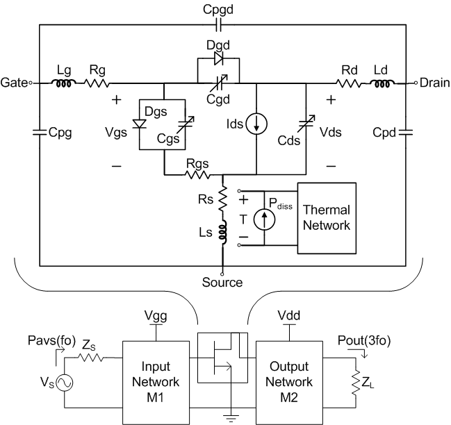
Fig. 1 Single-ended frequency tripler topology and nonlinear model.
III. Frequency Tripler Design
The design of the frequency tripler is described in this section. The key design steps consist of the device biasing, the determination of optimal harmonic terminating impedances, and the synthesis of those impedances into realizable networks. A fundamental frequency of fo=3.33GHz is used for the 10GHz GaN HEMT-based frequency tripler.
A. Device Biasing
The fundamental concept of harmonic generation is to drive the device such that its output drain current waveform becomes clipped due to the transition between operating regimes. According to Fourier analysis, a symmetrically-clipped drain current waveform is desirable in the case of a frequency tripler due to its rich odd harmonic content. The two hard nonlinearities which create this clipping effect are delineated by the pinchoff regime and the forward conduction of the gate-source diode. The ease with which the waveform is clipped and the amount of symmetry is determined primarily by the device bias, drive level and terminating impedances at each harmonic.
Double-sided clipped waveform analysis has shown that the optimum bias condition for third harmonic generation is midway between forward conduction and pinchoff [15]. Low power devices which do not suffer from significant self-heating can be conveniently biased in this manner; however, in the case of the GaN HEMT device, the IV characteristics change as a function of the dissipated power. This varies with the quiescent bias and dissipated power level as shown in the pulsed-IV (PIV) characteristics of Figs. 2. Therefore, selection of the gate bias is not a trivial choice and should be chosen utilizing extensive simulations of the output power level with respect to the gate-biasing. The bias which provides the maximum 3fo output power has been determined to be Vgs=‑2.3V with a drain bias of Vds =28V.
GaN HEMT devices are particularly well suited for third harmonic generation at the higher frequencies because they possess (1) a relatively high pinchoff voltage as compared with SiC MESFET devices and (2) a high fT unity gain frequency. A high pinchoff voltage allows the drain current to clip with less voltage swing at the gate. A high fT frequency allows the 3fo harmonic generated at the input to be delivered to the output.
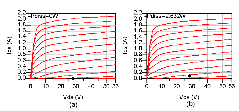
Fig. 2 Simulated PIV characteristics of the GaN HEMT model at a bias of (a) Vgsq=-3.0V, Vdsq=28V and (b) Vgsq=-2.3V, Vdsq=28V.
B. Determination of Input and Output Harmonic Terminations
Once the application of the optimal bias level is established, proper load and source impedances are applied to achieve increased gain and output power. Harmonic load and source-pull simulations are performed on the nonlinear model to determine the optimal impedances for maximum 3fo generation. Figure 3 shows the overall simulation setup. This simulation is unique in that it employs ideal triplexer components which permit the separation and independent tuning of the harmonic impedances seen by the device at both the input and output ports. This is an extension of the concept employed in [9] in that three harmonics are now considered instead of two.
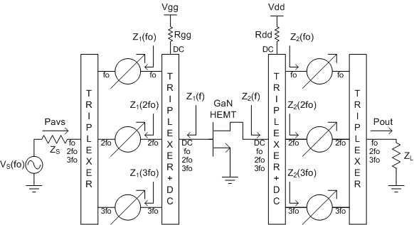
Fig. 3 Generalized harmonic load and source-pull simulation setup used for the analysing the power of the GaN HEMT device.
This generalized method is advantageous in that the effect of each harmonic load can be explored independently since the configuration assumes no particular topology. Once the harmonic impedances are determined, the designer can choose one of many possible realizations of the networks. For the source network, an impedance match at fo and harmonic reflectors for 2fo and 3fo are desirable for increasing the overall gain and output power. Likewise, for the load network, an output match at 3fo provides increased power while harmonic reflectors for 1fo and 2fo provide increased gain, power and suppression of the undesirable harmonics.
The harmonic impedance values determined from this analysis that result in producing the maximum 3fo power are plotted in Fig. 4.
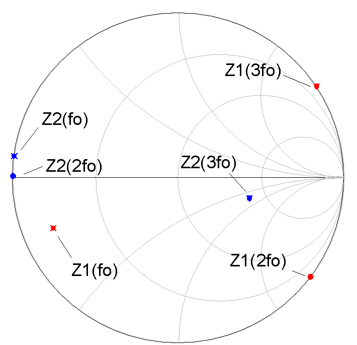
Fig. 4 Harmonic load and source impedances determined from simulation
C. Synthesis of Input and Output Networks
This prototype design uses external bias tees and, therefore, attention will be focused on the design and implementation of the microwave load and source networks. The major challenge in building a frequency tripler is realizing an output network such that a short circuited fundamental reflector does not inadvertently short circuit the desired third harmonic signal. Several authors have used combinations of transmission line (TL) and lumped elements [17],[19],[20], filters [11], coupled lines [2] and novel composite right-hand/left-hand TLs [13] to solve this problem.
One goal in the synthesis and fabrication of the harmonic networks is to minimize circuit and substrate losses. Thus the resulting topology is kept as simple as possible. The design presented here, shown in Fig. 5, utilizes a cascaded harmonic network using short feed lines at the input and output and quarter-wavelength harmonic impedance reflectors where possible. The input network consists of a matching stub for fo and reflectors for the 2fo and 3fo harmonics. The output network consists of a 2fo reflecting stub followed by a fundamental-rejecting coupled line section and 3fo matching stub. The authors have chosen to use a coupled line to pass the third harmonic, while rejecting the fundamental.
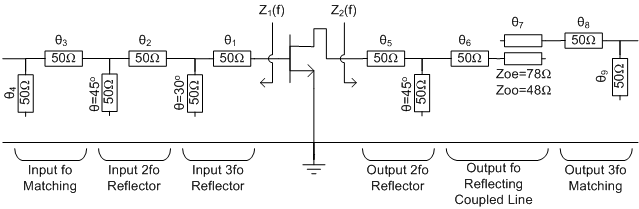
Fig. 5 Circuit topology of GaN frequency tripler prototype
The input and output networks shown in Figure 4 were fabricated in Rogers RT/Duroid 5880 substrate. The choice to use 50 ohm lines for all the transmission line elements is dictated by the necessity to avoid excessive heating of the microstrip traces resulting from high power reflection.
IV. Measurement and Performance
The output power of the frequency tripler was measured in a large-signal test setup capable of delivering up to +39dBm of available power.
The harmonic output power and conversion gain of the GaN HEMT frequency tripler is shown in Figs. 6 and 7, respectively. The measured output shows that the realized circuit is capable of producing 30.0dBm (1.0W) output power and 2.9dB conversion loss at the third harmonic. The simulated output closely predicts the measured 3fo harmonic over a reasonable range of available powers (Fig. 6). Conversion loss (Fig. 7) is also estimated closely over a useful range of available powers.
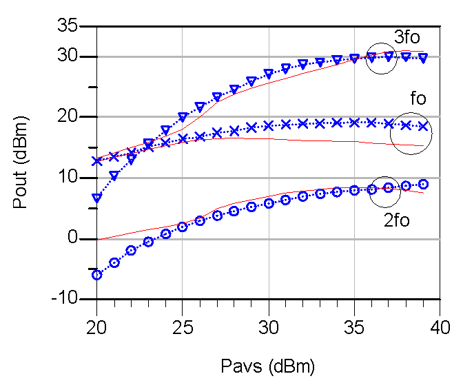
Fig. 6 Measured and simulated output power for the frequency tripler for three harmonics.
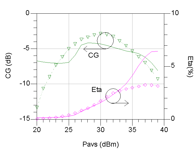
Fig. 7 Measured and simulated conversion gain and efficiency of frequency tripler.
A comparison table between this work and recently published frequency triplers is shown in Table I. The table summarizes the maximum performance reported in each of the publications. According to the table, the frequency tripler design presented here represents the highest output power, single-transistor tripler available to date producing over 50 times more power than that of the next highest.
TABLE I
Comparison of Recently Published Triplers
| Work | 3fo
(GHz) |
CG
(dB) |
Pout
(dBm) |
η
(%) |
Pout1fo/Pout2fo
(-dBc) |
| This | 10 | -2.9 | 30.0 | 3.14 | -11.2/-21.8 |
| [2] | 7.5 | -2.4 | 1.6 | 13 | -33.6/-29.6 |
| [4] | 38.64 | -2.7 | 4.7 | 11 | -38/-23 |
| [5] | 140 | -11 | -1.5 | — | —/— |
| [11] | 34.5 | -6.5 | -6.5 | — | —/— |
| [12] | 3 | 5.5 | 6 | 57 | <-25/<-25 |
| [13] | 3 | -5.67 | -5.67 | — | -62.72/-53.6 |
| [14] | 9 | 2.9 | 12.9 | 7.5 | -28/-28 |
| [15] | 42-51 | — | 12.5 | — | -40/-20 |
| [16] | 6 | 0.5 | 6 | — | -50/-19 |
| [17] | 2.475 | 9 | 12 | 22.5 | —/— |
| [18] | 30 | -5 | 12 | 5 | <-50/<-40 |
| [19] | 8.85 | 2.9 | 7.9 | — | <-35/<-50 |
| [20] | 8.82 | 3.67 | 9.17 | — | -28.67/-26.87 |
V. Conclusions
A GaN HEMT-based frequency tripler producing a maximum output of 30.0dBm and -2.9dB conversion gain has been demonstrated. The design of the frequency tripler was performed using harmonic load-/source-pull simulations utilizing a high-precision nonlinear device model. Frequency multiplication techniques using impedance matching at the desired harmonics and reflection at unwanted harmonics allow increased output power while minimizing conversion loss.
Acknowledgment
The authors wish to acknowledge Dr. Wayne Martin and Dr. Giovonnae Anderson for their support and Swapnil Jain for his technical assistance.
References
[1] F. Ghannouchi, R. Larose, and R.G. Bosisio, “A New Multiharmonic Loading Method for Large-Signal Microwave and Millimeter-Wave Transistor Characterization,” IEEE Trans. Microwave Theory & Tech., vol.39, no.6., pp.986-992, June 1991.
[2] D.L, Le, F.M. Ghannouchi, R.G. Bosisio, “A Novel Approach for Designing GaAs FET Frequency Multipliers with Optimum Conversion Gain and Power Efficiency,” Microwave & Optical Tech. Letters, vol. 5, no. 9, pp. 403-408, August 1992.
[3] B. Thibaud, D. Barataud, M. Campovecchio, J.M Nebus, S. Tranchant, P. Quentin, and D. Floriot, “CAD Oriented Design Methods of Frequency Multipliers. Application to a Millimeter Wave PHEMT Tripler and a Microwave HBT Doubler,” 1999 IEEE MTT-S Digest, pp. 1747-1750, 1999.
[4] A. Boudiaf, D. Bachelet, C. Rumelhard, “A High-Efficiency and Low-Phase-Noise 38-GHz pHEMT MMIC Tripler,” IEEE Trans. Microw. Theory and Tech., vol. 48, no. 12, pp. 2546-2553, Dec. 2000.
[5] Y. Campos-Roca, C. Schwörer, A. Leuther, and M. Seelmann-Eggebert, “G-Band Metamorphic HEMT-Based Frequency Multipliers,” IEEE Trans. Microwave Theory & Tech., vol. 54, no.7, pp. 2983-2992, July 2006.
[6] Y. Abe, R. Ishikawa, K. Honjo, “Inverse Class-F AlGaN/GaN HEMT Microwave Amplifier Based on Lumped Element Circuit Synthesis Method,” IEEE Trans. Microw. Theory and Tech., vol. 56, no. 12, pp. 2748-2753, Dec. 2008.
[7] M. Helaoui, and F. M. Ghannouchi, “Optimizing Losses in Distributed Multiharmonic Matching Networks Applied to the Design of an RF GaN Power Amplifier with Higher Than 80% Power-Added Efficiency,” IEEE Trans. Microw. Theory and Tech., vol. 57, no. 2, pp. 314-322, Feb. 2009.
[8] Y. Chung, K. M. K. H. Leong, and T. Itoh, “AlGaN/GaN HEMT X-band frequency doublers with novel fundamental frequency reflector scheme,” IEICE Trans. Electron., vol. E86-C, no. 8, pp. 1416-1421, 2003.
[9] K. S. Yuk, G. R. Branner, and C. Wong, “High Power, High Conversion Gain Frequency Doublers using SiC MESFETs and AlGaN/GaN HEMTs,” to be published in Proc. IEEE MTT-S Int. Microw. Symposium, May 2010.
[10] K. S. Yuk, G. R. Branner, and D. J. McQuate, “A Wideband, Multiharmonic Empirical Large-Signal Model for High-Power GaN HEMTs With Self-Heating and Charge-Trapping Effects, IEEE Trans. MTT, Vol. 57, No. 12, pp. 3322 – 3332, Dec. 2009.
[11] G. Zhang, R.D. Pollard, and C.M. Snowden, “A Novel Techinique for HEMT Tripler Design,” 1996 IEEE MTT-S Digest, pp. 663-666, June 1996.
[12] E. Sandhiya, D. Denis, and I.C. Hunter, “Novel Design Methodology for High Efficiency Class E Microwave Frequency Triplers,” in Proc. IEEE MTT-S Int. Microw. Symposium, pp. 1825-1828, June 2006.
[13] S. Seo, Y. Jeong, J. Lim, B. Gray, and J Stevenson Kenny, “A Novel Design of Frequency Tripler Using Composite Right/Left Handed Transmission Line,” IEEE MTT-S Int. Microw. Symposium, pp. 2185-2188, June 2007.
[14] W. Ciccognani, E. Limiti, P. Longhi, and L. Scucchia, “Harmonic Matching Design for Triplers,” Integrated Nonlinear Microwave and Millimetre-Wave Circuits 2008, pp. 141-144, November 2008.
[15] H. Fudem and E.C. Niehenke, “Novel Millimeter Wave Acdtive MMIC Triplers,” 1998 IEEE MTT-S Digest, pp. 387-390, 1998.
[16] B. Bunz, and G. Kompa, “Broadband HEMT-based Frequency Tripler for Use in Active Multi-Harmonic Load-Pull System,” 34th European Microwave Conference, Amsterdam, pp.193-196, 2004.
[17] Y. Park, “Class-F Technique as Applied to Active Frequency Multiplier Designs,” IEEE Trans. Microw. Theory & Tech., vol. 57, no.12, pp. 2983-2992, Dec. 2009
[18] C. Beaulieu, “Millimeter Wave Broadband Frequency Tripler in GaAs/InGaP HBT Technology,” IEEE MTT-S Digest, pp. 1581-1584, 2000.
[19] J.P, Mima, and G.R. Branner, “Synthesis of Active Microwave Frequency Triplers,” Proc. 43rd IEEE Midwest Symp. On Circuits & Systems, pp. 20-22, August 2000.
[20] J.E. Johnson, G.R. Branner, and J.P Mima, “Design and Optimization of Large Conversion Gain and Active Microwave Frequency Triplers,” IEEE Microwave & Wireless Components Letters, vol. 15, no. 7, pp. 457-459, July 2005.
[21] “CGH40010 10W, RF Power GaN HEMT datasheet Rev. 1.3 – March 2007,” Cree, Inc., Durham, NC, 2007. [Online]. Available: http://www.cree.com/products/pdf/CGH40010.pdf.