

 0
0
 0
0
By K.W. Current, K. Yuk, C. McConaghy, P.R.C. Gascoyne, J.V. Vykoukal, C. Andrews
Originally appears: IEEE Transactions on Biomedical Circuits and Systems, Volume 1, Issue 2, pp. 105 – 115, Jun. 2007.
A high-voltage (HV) integrated circuit has been demonstrated to transport fluidic droplet samples on programmable paths across the array of driving electrodes on its hydrophobically coated surface. This exciter chip is the engine for dielectrophoresis (DEP)-based micro-fluidic lab-on-a-chip systems, creating field excitations that inject and move fluidic droplets onto and about the manipulation surface. The architecture of this chip is expandable to arrays of NxN identical HV electrode driver circuits and electrodes. The exciter chip is programmable in several senses. The routes of multiple droplets may be set arbitrarily within the bounds of the electrode array. The electrode excitation waveform voltage amplitude, phase, and frequency may be adjusted based on the system configuration and the signal required to manipulate a particular fluid droplet composition. The voltage amplitude of the electrode excitation waveform can be set from the minimum logic level up to the maximum limit of the breakdown voltage of the fabrication technology. The frequency of the electrode excitation waveform can also be set independently of its voltage, up to a maximum depending upon the type of droplets that must be driven. The exciter chip can be coated and its oxide surface used as the droplet manipulation surface or it can be used with a top-mounted, enclosed fluidic chamber consisting of a variety of materials. The HV capability of the exciter chip allows the generated DEP forces to penetrate into the enclosed chamber region and an adjustable voltage amplitude can accommodate a variety of chamber floor thicknesses. This demonstration exciter chip has a 32 x 32 array of nominally 100 V electrode drivers that are individually programmable at each time point in the procedure to either of two phases: 0 and 180 with respect to the reference clock. For this demonstration chip, while operating the electrodes with a 100-V peak-to-peak periodic waveform, the maximum HV electrode waveform frequency is about 200 Hz; and standard 5-V CMOS logic data communication rate is variable up to 250 kHz. This HV demonstration chip is fabricated in a 130-V 1.0um SOI CMOS fabrication technology, dissipates a maximum of 1.87 W, and is about 10.4 mm x 8.2 mm.
I. Introduction
As microelectronics fabrication technology scaling and integrated device performance improve, the realization of a “laboratory on a chip” for chemical and fluid analysis becomes more feasible. A microscale fluidic analysis device could be portable, robust and durable, store samples and chemicals in well controlled spaces that have reduced exposure to environmental contamination, use highly accurate metering of small quantities of reagents and samples, be time efficient through parallel processing, and be cost efficient with small-quantity sample and chemical usage. The hardware may be of a disposable or a reusable type. It could provide wider availability of valuable diagnostic tools, reduce costs of chemicals and samples due to volume scaling, and provide versatility by testing multiple agents with a generic fluidic analyzer type.
Such a microfluidic analysis system has many potential applications in public health, medicine, and chemical and biological fluid analysis. It can potentially be used to detect chemical agents (pollutants and poisons) in water and in bodily fluids, and to characterize cells based on, for example, their distinct dielectric properties.
One of the emerging methods of performing fluid analysis uses dielectrophoresis (DEP)-based forces to move droplets within a fluid medium by subjecting them to inhomogeneous electric fields. Simple precise control of droplet movement within a reaction chamber by electronic means would be an important attribute of a microfluidic analyzer. Sensing droplet location and cell and chemical characteristics by electronic means would also be highly desirable.
The application of DEP to droplet manipulation has become more popular and numerous devices using planar microelectrode arrays employing DEP have been developed in recent years [e.g., 2, 3, 4]. The biphase programmable 320 320 array of 20 m actuation electrodes described in [2] has been shown to move, trap and separate individual cells in a parallel fashion using DEP forces and provides optical detection of individual cells. In this device, droplets are levitated between the microchamber lid and the electrode array in a sealed environment and are manipulated using electrode voltages of only 3.3–6.6 V. A planar, checkerboard patterned array of 741 10 m circular electrodes capable of creating arbitrary electric fields using sample and hold circuitry is introduced in [3], but its droplet manipulation capability has not been verified. A cell separator in [4] using a combination of fluid flow and DEP induced movement generated by a planar microelectrode array implements a cell fractionation technique which has verified that cells of the same type experience a constant force independent of position and that different cells can be separated based on their dielectric properties. However, this device’s need for a fluid flow source may complicate implementation hardware. Determination of chemical and cell characteristics by electronic means using microliter volumes, such as the sorting of cancer cells, has been demonstrated [5]. Other examples of the application of these specific ideas have also been reported, for example [9]–[11]. The integrated circuit (IC) engine presented here is designed for maximum flexibility in handling a wide variety of microfluidic operations and includes electrode excitation voltages that can be set to any value between nominally 3.3–130 V at a wide range of frequencies. This unique capability of the excitation engine allows an enormous range of possible cells, molecules, and fluidic manipulations to be used within a reaction chamber, and also allows a wide variety of fluidic reaction chamber configurations to be used.
In this paper, we present a high-voltage (HV) electrode exciter IC that can serve as the general purpose engine for general-purpose microfluidic analyzer systems. We also discuss a prototype programmable fluidic processor (PFP) system that utilizes this electrode exciter chip and its constituent parts. The PFP electrode exciter chip has been demonstrated manipulating droplets of nanoliter volumes across its surface in a precisely-controlled manner [7], [8].
Section II gives an overview of the concept behind the manipulation of droplets by DEP forces and characterization based on dielectric properties of the droplet sample. Section III describes the concept, specifications, and objectives of the prototype demonstration PFP system, its constituent parts, and its electrode exciter chip engine. Section IV discusses the electrode exciter chip architecture and operation. This includes the communications components needed to program the phase configuration of the electrodes, the HV biphase drivers at each electrode site and the additional circuitry implemented at select electrode sites for DEP-assisted droplet injection. The experimental performance of electrode exciter chip is presented in Section V. A summary and conclusions are presented in Section VI.
II. Fundamentals of Dielectrophoresis
DEP forces can induce movement of uncharged but polarizable particles under the influence of an inhomogeneous electric field [1]. In positive DEP, a polarizable particle within a non or less polarizable medium is polarized in the direction of an applied inhomogeneous electric field, creating a greater net force and movement towards the higher electric field gradient. In negative DEP, the particle is non or less polarizable than its surrounding medium, causing the particle to be pushed away from the higher electric field gradient.
DC electric fields can be used to generate DEP forces, but ac electric fields are preferred to exploit the frequency-dependent dielectric properties of particles and cells. The polarization direction of the particle’s charges exhibits an ac behavior when subject to an ac electric field. However, the resulting force can vary depending on the frequency and dielectric properties of the particle. The time averaged DEP force experienced by a particle can be expressed by

where eps_m is the permittivity of the medium, a is the radius of the particle, Erms is the electric field and Ke is the Claussius Mosotti factor, representing the complex permittivities of the particle [1], [3], [4]. The contribution of the complex permittivities of the particle, eps_p* , and of the medium, eps_m*, are contained in Ke, which can be expressed by

where
![]()

where is the permittivity and is the conductivity of the particle or suspending medium, and is the applied ac frequency. Therefore, the DEP force experienced by the particle and thus its movement in response to that force is a function of the frequency dependent dielectric properties of the particle as shown in (1), [1], [6]. In theory, by exploiting this relationship, the movement response of a particle subjected to a known electric field in a known medium can be used to characterize the particle based on its unique dielectric behavior. Likewise, an unknown particle subject to the same applied fields can be identified using the movement response data from known particles.
DEP, electrowetting, and other related concepts are alternative perspectives on a single mechanism. Their comparisons and contrasts require subtle distinctions and complicated evaluations that are beyond the scope of this paper.
In the next section, the characteristics of a general purpose fluidic processor are discussed.
III. Programmable Fluidic Processor System
Droplet-based programmable microfluidic processors promise to offer solutions to a wide range of applications in which chemical and biological analysis and/or small-scale synthesis are required. Such devices will become the microfluidic equivalents of electronic microprocessors by offering off-the-shelf solutions for almost any fluid-based analysis or synthesis problem. A general-purpose droplet processor should be able to manipulate droplets of different compositions (including those that are electrically conductive or insulating and those of polar or nonpolar nature), to control reagent titrations accurately, and to remain free of contamination and carry over on its reaction surfaces.
The PFP, a fluidic analog of a microprocessor, employs dielectrophoretic forces through voltage excitations that move chemical and biological droplets of varying sizes and types within a two dimensional manipulation surface. Electric field excitations are controlled by metal electrodes that lie underneath the droplet manipulation surface. Equipped with a program memory, the PFP can execute simultaneous movement of multiple droplets or biological cells along precise arbitrary paths within the array of identical electrodes. By utilizing the ability to move droplets by non-mechanical means, simple chemical reactions as a result of droplet mixing can be performed. In this operation, two or more droplets of differing types are transported to the same array location and combined, creating a product that is indicative of characteristics of the original samples. The resulting droplets can then be transported to locations on the array for characterization. Likewise, a single droplet composed of several constituents can be separated into several droplets based on its electrochemical properties. Other advantages of a programmable array are the ability to functionally divide the exciter array so that several droplets can be handled in parallel and the ability to logically group multiple electrodes in order to handle larger droplet volumes.
In addition to manipulation of droplets on the reaction surface, a means that allows controlled injection of droplets from an external reservoir onto the reaction plane and an electronic droplet sensing scheme for droplet locating are desirable elements in a complete fluidic system.
In a prototype programmable PFP, a MEMS microfabricated fluidic reaction chamber containing an inert fluid medium such as bromododecane [1] is mounted atop the electrode exciter chip and serves as the arena for two-dimensional droplet manipulation. The conceptual operation of the fluidics processor is as follows. A fluidic sample is injected into the medium-filled chamber through microfluidic channels in a controlled manner by DEP-assisted droplet injection. After the desired sample quantity is collected at a desired electrode location, the adjacent electrodes are excited by programmed commands to facilitate sample movement in the reaction chamber above the electrode excitation chip. After manipulation of the droplets is complete, the sample and medium are flushed out of the chamber area and replaced with fresh medium for the next analysis.
The signals required to operate the exciter chip originate in a software application that records the desired movements of multiple droplets over time. This information is encoded and routed from a programmable digital assistant (PDA) through an electronic interface that sends the appropriate information to be loaded into the memory of the electrode exciter chip. The exciter chip memory contains information to define the present droplet locations and the next droplet locations. Chip memory is updated for droplet locations at each time point.
The prototype PFP analyzer is composed of the MEMS fluidic chamber, the electrode exciter chip, an interface board for producing the electrode exciter chip control signals and interfacing with a personal digital assistant (PDA), and desktop PC software used to program the PDA with the desired droplet movement path. The PC software will migrate into the PDA, eliminating the need for a PC.
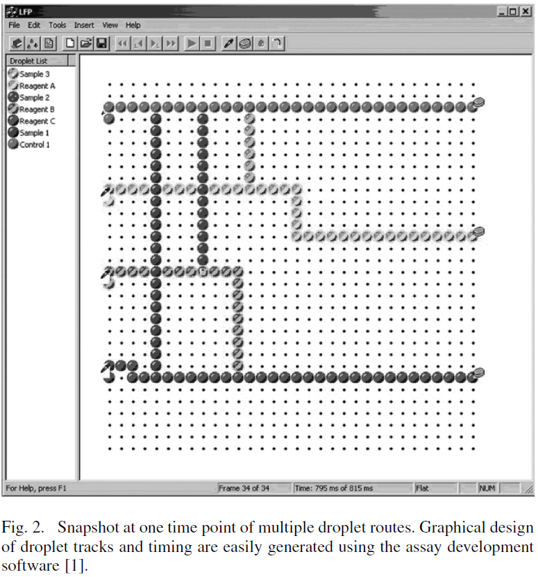
The block diagram of the entire PFP system and its support is shown in Fig. 1 [1]. Indicated in the left-hand side of the diagram is an Assay Development Host Computer that runs a user interface designed to create a sequence of commands that will be implemented by a personal digital assistant (PDA) and the electrode excitation IC engine described later. The assay development software gathers information about the fluids that will be in the sample and reagent chambers, the quantities of the fluids to be moved and combined, the time sequence of movements by the fluid droplets, sequence of combining of fluids, droplet splitting, droplet movement to the result sensors, droplet movement to the waste chambers, and other information necessary to control the PFP. Assay design templates help the user stay within practical timing, droplet volume, and other limitations inherent in the microfluidic system hardware. Multiple parallel injection operations and simultaneous multiple droplet movements are easily accommodated. Combining droplets is implemented by placing droplets at the same place at the same time. Fig. 2 [1] illustrates one time point in a graphical droplet routing window used to design droplet movement on the PFP electrode array. The simulation of droplet behavior during the entire assay time can be viewed. The completed assay procedure is then compiled into commands that will be implemented by PFP software that runs in the PFP PDA controller. The compiled PDA commands for the entire assay are then transferred to the PDA as indicated in Fig. 1. The PDA then controls the PFP at each step of the assay. In the demonstration system we have evaluated, a signal conditioning board provides the proper signal levels and types to the electrode exciter chip for each PDA control signal.
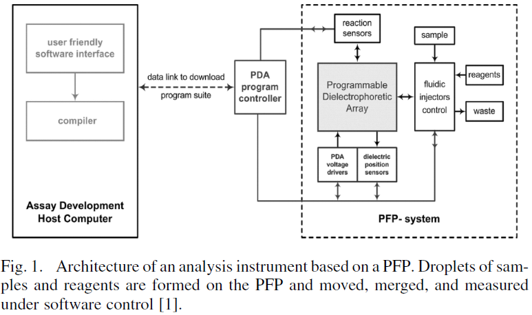
The block labeled “Programmable Dielectrophoretic Array” shown in the PFP system block diagram in Fig. 1 is the HV electrode exciter IC engine to be described later. The IC is mounted in a microfluidic MEMS structure that has several fluid reservoirs, and their corresponding channels that lead fluids to the reaction surface. A single type of electrode exciter IC engine can be used with different organizations of the MEMS fluid structures. A variety of techniques may be used to help control fluid injection and drop size, and at present, optical sensing of droplet location and reaction results is used in the demonstration configuration characterized for this presentation. Electronic droplet location and reaction results sensing are now in development. The blocks within the “PFP-system” area of Fig. 1 indicate a typical implementation of the MEMS structure. Variations are easily introduced.
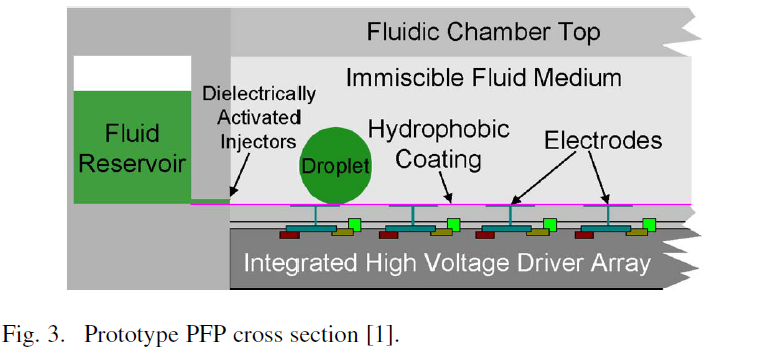
 The PFP electrode driver chip and MEMS structure cross section is illustrated in Fig. 3 [1]. The MEMS structure holds the fluid reservoirs and the fluid microchannels, and seals the bottom (and edges, if necessary) of its reaction chamber (the open area of the MEMS structure directly above the chip electrode array) to the top surface, the passivation layer, of the CMOS chip. Silicon, glass, plastic and other materials may be used to construct the MEMS structures. MEMS reaction chambers may have bottom layers of various thicknesses, or as demonstrated in this presentation, the chip itself may be used as the reaction surface. In this demonstration PFP, the chip’s passivation layer is coated with a thin microroughened layer of hydrophobic coating that prevents droplets from sticking and immobilizing against the surface, to prevent wetting, and to prevent contamination of the droplet movement surface [1]. The reaction chamber is filled with an inert, insulating oil, such as bromododecane. The fluid reservoirs have injection channels that open in the oil-filled reaction chamber. The sample fluids and test chemicals are loaded into the reservoirs and then injected into the reaction area with assistance by DEP forces [1]. The driver electronics for each electrode site lie directly beneath the respective electrode.
 The versatile capabilities of the PFP analyzer system are designed into the PFP electrode exciter chip. The electrode size was selected to be 100 m on the top metal layer each separated by 100 m, in a regular array, based upon DEP and fluid properties [1]. The chip architecture allows arbitrary expansion of the electrode array in both directions of the array on-chip. This also allows easy connection in groups of chips to provide larger droplet manipulation surfaces. The demonstration chip uses a 32 x 32 array of electrodes, identical HV electrode driver circuits, and the appropriate standard CMOS logic.
The PFP electrode array generates the forces for DEP droplet manipulation. Each electrode driver in the array can be programmed to produce either a 0 (in-phase) or 180 (out-of-phase) phase delayed square-wave. The 180 phase shift results in an electric potential between adjacent electrodes and an electric field across the inter-electrode space. The electrode geometry is contoured to make the E-field spatially inhomogeneous giving rise to the DEP force. An ac waveform is necessary to exploit the frequency-dependant properties of the sample, while HV may be necessary for correct actuation in environments exposed to shock and varying orientations, or for certain molecules and cells with certain mass and volume. The array’s phase configuration produces controlled inhomogeneous electric fields between adjacent sites confining a droplet to a particular electrode site or transporting it between sites [1]. For example, a fluid droplet will stay atop an in-phase electrode if the surrounding electrodes are out-of-phase. However, if an adjacent electrode is changed to in-phase and the residing electrode is changed to out-of-phase, the droplet will move away from the out-of-phase electrode towards the in-phase one. PFP array programming configures the electrodes’ signal phases, resulting in precise droplet manipulation along a defined path, sectioning of the array for parallel manipulations, and grouping of multiple electrodes for handling larger droplet volumes and combining or separating droplets [1]. The prototype electrode exciter chip is described below.
IV. High-voltage CMOS electrode exciter chip
Prototypes of HV electrode exciter chips were fabricated in a 1um SOI CMOS technology that has one layer of polysilicon and three metal layers. Metal layer 3 is used for the electrodes only. Signal and power are routed on metal 1, metal 2, and poly. The technology is specified with 130-V breakdown. CMOS logic levels down to 3.0 V are supported.
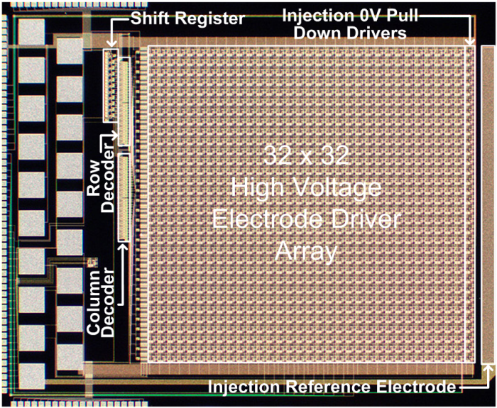
Fig. 4 [8] shows the 32 32 demonstration PFP chip architecture. It has an array of HV electrodes and electrode driver circuits that contain the array memory, and communication-related functions that are standard CMOS logic. The communications circuitry consists of an 11-bit communications shift register (SR) with gated outputs, and a 5-bit row decoder, and a 5-bit column decoder for programming the array memory.
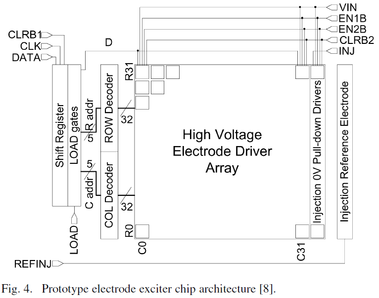 Each HV electrode driver “cell” occupies a 200 m area that contains the electrode driver electronics and the 100 m area top metal layer, metal 3 (M3), “pixel” electrode centered within the driver cell. The electrodes have a pitch of 200 m in both directions. Each electrode driver cell has memory for storing its present and next phase state data.
In addition to the HV array driver cells, DEP-assisted injection electronics and the injection reference electrode are shown at the right of Fig. 4. The injection electronics connect to the rightmost (in the figure) column of HV electrodes and are composed of a column of programmable HV pull down drivers with memory that allow the last column of HV array electrodes to maintain a voltage state close to ground as long as the injection command is asserted. The injection reference electrode that runs the entire distance of an array column under the fluid injection channels and the injection electronics for each element in the injection edge column of array electrodes provide a potential difference at the injection channel tips to control droplet formation.
The communications circuitry consists of an 11-bit communications SR, a 5-bit row decoder, a 5-bit column decoder and signal buffers for some of the intermediate lines. The shift register stores a sequence of bits representing the row address, column address and desired phase state for programming. A bank of eleven 2-input AND gates at the shift register outputs provides control over the propagation of the data from the SR to the decoders. The decoders are used to decode the binary addresses stored in the shift register and enable the targeted row or column line. To increase the driving capability at heavily loaded nodes, inverter buffers (not shown in Fig. 4) are placed between the gated shift register outputs array’s phase data input line, between the gated shift register output and decoder inputs for the address data, and between the decoders and the array for the row and column lines.
A communication transaction loads one new entry into a single location in the array memory. For any desired motion of droplets between present and future locations, the array memory must be loaded with the necessary pattern of phase differences to accomplish the droplet movement when the next time point is activated. This may be as few as one new phase or as many as hundreds of new phases may be required. Configuring the phase outputs of the electrode array begins by selecting and storing the next state data of each desired array site. First, the 5-bit column address of the first target cell is clocked into the communications shift register through DATA IN followed by the 5-bit row-address and finally the 1-bit phase state data. The shift register reads in a new data bit for every strobe of CLK. Once the data vector is completely loaded into the shift register, the LOAD signal is enabled allowing the shift register outputs to pass the addresses to the decoders and the new phase data bit to the array cells. The decoders translate the binary addresses and apply a logic high signal to the corresponding row and column lines, enabling the targeted cell’s memory to latch the new phase data. At the same time, the phase data bit is sent from the shift register to the data input lines of all driver cell memories. When EN1B is pulsed from high to low, the new data is stored into the input latch of the target cell’s two-stage latch memory without modifying the current output phase state. The sequential programming process is repeated for every desired driver cell. Once the desired pixel next state updates are complete, EN2B is pulsed from high to low and the data in the output latch of the driver memories are updated with the data stored in the input latch. The data from the output latch sets the cell’s output phase and the array is simultaneously updated with the new output phase configuration.
The data presented here came from chips that used square waves on the HV electrodes and all-digital electronics to drive the electrodes. Square waves have substantial high frequency harmonics that can obscure the characteristic impedances of some samples. Analog circuitry for generating sinusoidal electrode excitations has been fabricated in electrode arrays and characterized. Its performance, as an analog circuit, is more sensitive to the variation of the chip fabrication technology parameter variation than the digital circuit performance. The analog circuits can generate both sinusoidal and square wave electrode excitations. As PFP system performances are characterized in various applications, it may be determined that analog electrode drivers may be more desirable or required for certain situations. Both analog and digital driver cells use the same enable and latching logic. The electronic design and chip cell layout on the prototype chip are organized so that the actual HV driver circuitry, either analog or digital, may be substituted directly, without further modification of the layout.
A. High-Voltage Electrode Digital Driver Cell
Each electrode has an underlying driver cell as shown in Fig. 5, [7] consisting of two D latches (DL) in master-slave flip-flop operation that store the phase data, addressing logic controlled by a row (ROW) line and a column (COL) line, and a HV electrode driver. The HV electrode driver consists of a 2:1 mux controlled by the flip-flop outputs C and CB, a HV nMOS transistor connected to the HV supply VHH through a 5-M load resistor and a M3 electrode connected to VOUT. The electrode output VOUT will be out-of-phase with the reference square wave VIN if C is logic low and in-phase if C is logic high. VIN sets the frequency of VOUT.
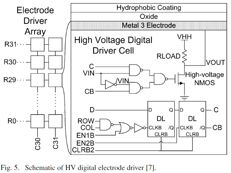 The electrode array’s next phase configuration is set by sequentially programming each site with the new phase data and then updating all phase outputs of the array simultaneously. A target driver is programmed by sending an 11-bit data sequence consisting of the 5-bit column address, 5-bit row address and 1-bit phase data into the DATA line of the SR controlled by CLK. After the data is set, addresses are passed to the decoders, and the phase data D is passed to the array cells by activating the gated output of the SR with the LOAD signal. The address enables only the target driver cell to accept the new phase data. When EN1B activates, the first DL of the target driver cell stores the new phase data from the D line and the memory is programmed. This entire programming sequence is repeated for each desired array cell. When all new data has been loaded, EN2B is activated, the second DL of each driver cell loads the new phase data and the output of the entire array is simultaneously updated with the new phase configuration.
The HV digital driver circuit is shown connected to the metal 3 electrode in Fig. 5 and consists of a HV nMOS (HV NMOS) pull-down transistor with a 5-M load resistor and a 2:1 NAND multiplexer. The drain of the HV nMOS is the output of the driver, VOUT, which drives the excitation electrode. The signal VIN is the low voltage square wave reference and VOUT is a HV square wave output with an output HV equal to VHH. The signals C and CB are taken from the driver memory output and set the phase of VOUT.
When gate of the HV nMOS is logic low, the HV nMOS turns off and VOUT pulls to VHH through RLOAD. Contrarily, when the gate is logic high, the HV nMOS turns on and pulls VOUT down to a voltage near ground. Periodically switching the gate of the HV transistor on and off will produce a square wave output at VOUT. At a peak output swing of 100 V, the peak output current will be 20 uA through the 5-M RLOAD when the HV transistor is turned on and pulling VOUT to a low voltage near ground. Therefore, the resistor loaded HV nMOS output driver has a static power dissipation of 2 mW during its on state.
The reference signal VIN controls the periodic output of the HV driver. The 2:1 input NAND gate multiplexer passes either VIN or its complement to the HV nMOS gate depending on C and its complement CB. When C is logic high,/VIN controls the HVNMOS gate, setting the output 0 in-phase with VIN. Contrarily, when C is logic low, VIN controls the HVNMOS gate and sets the output phase to 180 in-phase with VIN.
The memory enable logic and two-stage latch memory storing the phase state data at each electrode site are shown in Fig. 5. The input latch of the two-stage latch stores the next phase state data while the output latch maintains the current phase state at the output, allowing sequential programming and simultaneous updating of the array configuration. The signal EN1B enables the data input latch through the enable logic, while EN2B directly controls the output latch. The Q output of the dual latch is connected to the C input of the HV driver and the QB output is connected to the CB input of the HV driver.
The new phase data from the shift register is passed to all the array drivers at the input D. The memory latches D when CLKB is low, which occurs only when EN1B is logic low and both ROW and COL enables are logic high. Therefore, only the driver cell at the intended row and column location will receive the logic low EN1B signal through the enable logic, ensuring that only one driver cell can be programmed at a time. The active low asynchronous signal CLRB2 resets the dual latch output to logic low.
B. DEP-Assisted Droplet Injection Electronics
Fluid injectors are located to one side of the chip; their tips pass over the injection reference electrode with their tips close to the last column of electrodes in the array (COL31). In the injection scheme, a DEP force creating the supplemental pressure needed to bring fluid from the injector tip onto the chip surface is generated by a potential difference between a grounded electrode in the last column of the array serving as the collecting electrode and the injection reference electrode exerting an arbitrary signal.
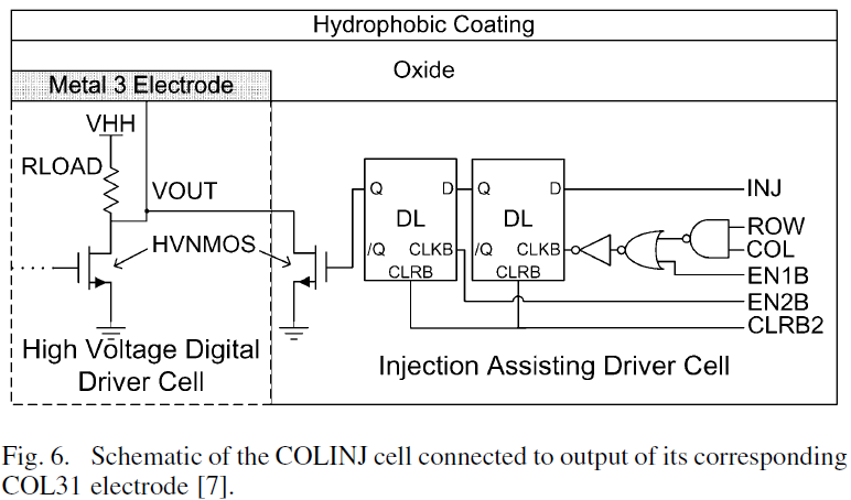
Any electrode in COL31 can be used for collection as each has a programmable injection driver, which pulls the output to a low dc voltage close to ground when activated. The injection driver circuitry is shown connected to its corresponding COL31 electrode in Fig. 6 [7] and is composed of a HV nMOS transistor, a flip-flop and addressing logic. Each injection driver shares the address of its adjacent driver cell but receives data from the INJ input. Programming an injection driver with a logic high INJ data turns on the HV nMOS transistor, which pulls the electrode output voltage near ground. The required signal can then be applied onto the injection reference electrode to induce droplet injection.
Fluid injectors fabricated within the MEMS chamber will be located at the right of the chip and overlap the reference electrode shown in Fig. 3, with tips pointing towards the right-most column of electrodes, COL31. In the proposed injection scheme, the DEP force creating the supplemental pressure needed to bring fluid from the injector tip onto the coated chip surface is generated by the electric field arising from the potential difference between an electrode in the last column serving as the collecting electrode and the reference electrode under the mounting location of the injector nozzle. This potential difference is created by activating the grounding electronics at the collection electrode site and externally applying the needed signal on the reference electrode.
The injector reference electrode provides a voltage close to the fluid in the injector tips so that an electric field can be generated between the collecting electrode and the injector fluid. The injection reference electrode is 300 um wide, spans the height of the array and is located 400 um to the right of the rightmost electrode column. It is composed of all conducting layers and its voltage is independently controlled through the external signal REFINJ. The optimum signal at REFINJ is externally connected and left flexible to allow for further study.
The electrodes in COL31, any of which can be used for droplet collection, can realize a third, near-ground output state through an additional column of programmable pull-down drivers referred to as the injection column (COLINJ). A COLINJ cell is composed of a pull-down HV NMOS, a 1-bit two-stage latch memory and addressing logic as shown in Fig. 6. Each COL31 cell is connected to a corresponding COLINJ cell at the electrode output and the two cells share the same array addresses and control signals. The COLINJ cell with pull-down HV nMOS is shown connected to the output electrode of the corresponding COL31 driver cell in Fig. 6. When the COLINJ HVNMOS is turned on, it pulls the electrode output towards ground regardless of the COL31 HVNMOS’s on/off state. The gate of the COLINJ HVNMOS is controlled by its own two-stage latch memory that receives data from an asynchronous externally supplied data signal, INJ. All COLINJ memories receive data from the INJ input rather than from the D phase data from the shift register.
To activate the near-ground voltage state, the address of the COL31 electrode site is loaded into the shift register and decoded into the corresponding enable lines in the normal fashion. When EN1B is pulsed, the matching COLINJ cell will store INJ into its own memory at the same time the COL31 cell stores D. If a logic high INJ data is latched, the COLINJ HVNMOS will turn on and pull the output of the COL31 electrode to ground when the array outputs are updated. However, if a logic low INJ is latched, the COLINJ HVNMOS will remain off and the COL31 cell will operate normally, producing a square-wave output with an output phase set by the COL31 cell’s phase data. Like the array driver cell memories, the COLINJ memories are also reset by the CLRB2 signal.
C. High-Voltage Analog Electrode Driver Circuit
An analog HV electrode driver was also fabricated and characterized. Both analog and digital HV electrode driver circuits use the same logic and memory. The differences are in generation of the actual HV signal on the electrode. The analog HV driver circuit schematic shown in Fig. 7(a) is a source-coupled binary phase-shift key (BPSK) circuit. The advantage of using an analog driver circuit is the ability to produce binary phase shifted sinusoids instead of square-waves, eliminating harmonic components present in the square wave. In addition, for use in capacitive sensing schemes, this basic structure can be reconfigured into the gain stage of a sense amplifier. However, the drawback of using the analog driver is the complicated current and voltage biasing required for all array drivers as well as the increased power dissipation from the constant current source.
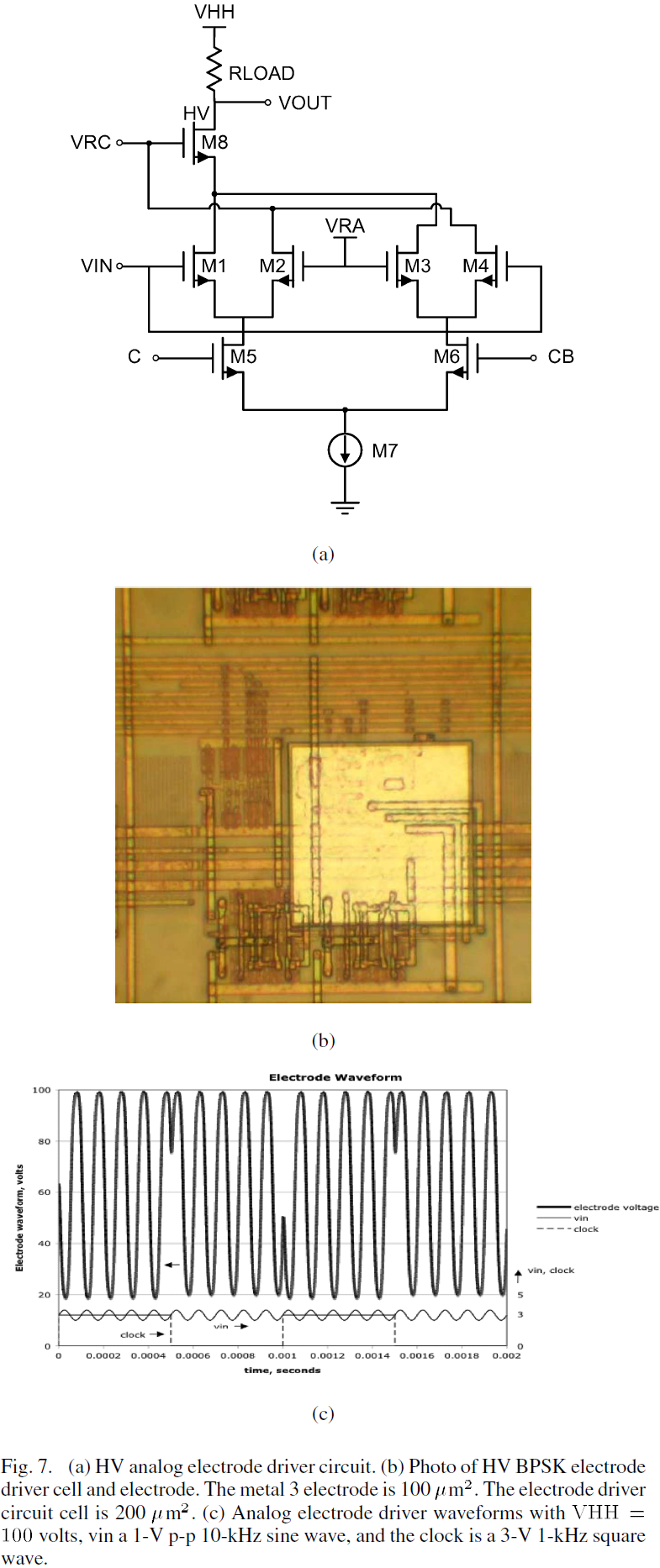 The analog driver circuit is composed of current-steering source-coupled pairs (M1–M6), a common gate HV nMOS transistor (M8), a load resistor, and a current source (M7). The analog cell operates as an analog multiplexer that passes control of VS8 to either a 0 or 180 phase shifted signal relative to the sinusoidal reference input VIN. The HV nMOS cascode transistor M8 allows the HV swing of the electrode driver circuit across its drain-source at the output VOUT, which is connected to the load resistor and the metal3 electrode.
The input of the circuit can be either single-ended or differential. In the single ended mode, VIN is the sinusoidal input reference of the circuit with a dc bias placing the transistors in saturation and VRA is a dc voltage equal to the bias of VIN turning on M2 and M3. In the differential case, VIN and VRA are both sinusoids but with opposing phase, biased at the same dc operating voltage. The voltage VRC turns M8 on and directly sets the dc bias of VD2 and VD4. VRC also sets the dc bias of VD1 and VD3 through a gate-source voltage drop of M8. Like the digital driver, the phase output of the analog driver depends on C and CB, the outputs of the phase state memory.
The BPSK circuit relies on current steering to operate as an analog multiplexer. When C is logic high and CB is logic low, M6 turns off, the differential pair M3-M4 is essentially off and the inputs to the differential pair M1-M2 determine VOUT. The source VS8 will be equal to VD1, which is controlled by the gate voltage VIN. When the sinusoidal amplitude at VIN is greater than VRA, more current is steered through M1 than M2, VS8 is pulled down and VOUT follows. When VIN is below VRA, more current is steering through M2 than M1 and VOUT is pulled up towards VHH through RLOAD. In this mode, the analog driver is producing a 180 phase shifted output. Contrarily, when C is logic low and CB is logic high, M5 turns off and the differential pair M3-M4 controls VOUT. The source VS8 is equal to VD3, which is controlled by the gate voltage VRA. When VIN is greater than VRA, more current is steered through M4 than M3 and the output voltage is pulled up to VHH through RLOAD. When VIN is below VRA, more current is steered through M3 than M4 and the output is driven down towards ground. Thus, the output phase follows the phase of VIN and the analog driver is producing a 0 phase shifted output.
A 20uA current source is provided by M7 that will give a 100-V peak-to-peak voltage drop across the 5-M resistor RLOAD. The average power dissipation for the analog driver is higher than that for the resistor-loaded digital driver because the 20uA current source is always on in the analog driver while the digital driver only consumes 20uA half of the period for a 50% duty cycle square wave.
Prototype analog electrode driver cells have been fabricated and characterized. Shown in Fig. 7(b) is a photo of one such cell. In the figure, the metal3 electrode is 100 m and is centered in the 200 m electronics cell. Shown in Fig. 7(c) are analog electrode driver circuit waveforms. The axis to the left is for the top waveform, the HV electrode voltage. The axis on the right is for the reference input voltage, vin, which, for this example, is a 1-V p-p 10 kHz sinusoid, and the 1-kHz (for this example) 3-V logical clock signal, C, the phase selection signal.
V. Experimental Performance of the Electrode Exciter Chip
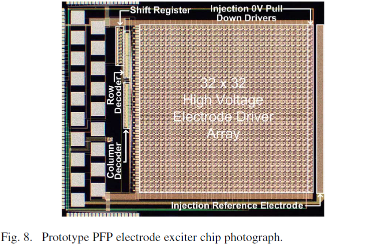
A photograph of the prototype PFP electrode exciter chip is shown in Fig. 8, [7] with the major regions identified. A 1.0-um 130-V high-resistance 1-poly 3-metal SOI CMOS fabrication technology is used. The die is approximately 10.4 mm x 8.2 mm. There are 19 large pads on the left side of the chip, which are to connect to an interface board through vertically mounted micro spring loaded pins. The other pads are standard wire bonding pads used for packaging test samples for electronic characterization.
 The communications and array circuitry of the prototype PFP electrode exciter chip are tested for functionality by observing the outputs at specific array locations during phase programming. Tests are performed at both low and high electrode excitation voltages to verify both logical functionality and HV performance.
The prototype PFP electrode exciter chip is tested for functionality at low output voltages by performing several programming cycles on the array driver cells and then updating the array phase outputs. Correct performance of the communications circuitry and the driver circuitry is demonstrated by addressing and changing the phase outputs of several electrodes. In addition, the COLINJ cell is programmed to activate, verifying the operation of the near-ground state output of the COLINJ electrode.
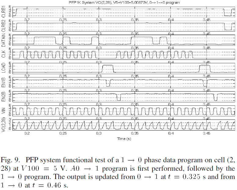
The programming of a driver cell to produce phase changes at its output is demonstrated. A driver cell is first programmed to perform an out-of-phase to in-phase output transition, followed by an in-phase to out-of-phase transition. The sequential phase changes correspond to programming the driver cell with a logic high phase data, followed by a logic low phase data. The experimental test waveforms of the driver cell at (2, 28) are shown in Fig. 9. The reset is deactivated at t=0.185 s and the eleven data bits composed of addresses and logic data are passed into the shift register from t=0.190 s to t=0.300 s. At time t=0.305 s, the LOAD signal is activated, passing the data from the shift register to the decoders and array, and at t=0.310 s, the EN1B signal is activated, commanding the target cell to latch in the logic high phase data. At t=0.325 s, the EN2B is activated and the output changes phases from out-of-phase to in-phase. Immediately following that, eleven new data bits targeting the same address but with a logic low phase data bit are loaded into the shift register from t=0.325 s to t=0.435 s. The LOAD signal is activated at t=0.440 s and EN1B is activated at t=0.445 s, latching the driver cell memory with a logic low phase data. At time t=0.460 s, EN2B is enabled a second time and the output square wave is updated with the logic low phase data, changing the output from in-phase back to out-of-phase with the VIN signal. At time t=0.475 s, the memory is reset, but the output of the digital driver is unchanged as it already contains a logic low phase data. The results show that the system is capable of programming a driver cell to both phases.
 Next, programming two drivers sequentially and updating their outputs simultaneously with memory reset is demonstrated. In the previous data, the EN2B signal is pulsed and the output updated immediately after the input latch of the target cell stores the input phase data. In this demonstration, two adjacent cells are sequentially programmed with a logic high data bit and then simultaneously updated once both cell memories have the new phase data stored in their input latches. The first cell is programmed with a logic high data bit and immediately after, another cell is programmed also with a logic high data bit. Only after the second cell is programmed is EN2B pulsed and the output of both programmed cells updated with the logic high phase data.
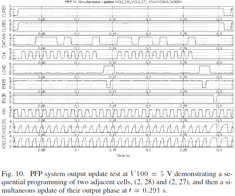
The two adjacent cells that are programmed sequentially and then updated simultaneously are at (2, 28) and (2, 27) and the test waveforms are shown in Fig. 10. At time t=0.017 s, CLRB1 and CLRB2 are set to logic high. The shift register receives the address and logic high phase data for cell (2, 28) between t=0.022 s and t=0.132 s. After that, LOAD is pulsed from t=0.137 s to t=0.153 s and EN1B is enabled from t=0.141 s to t=0.147 s, loading the logic high data into the cell’s input latch. From t=0.157 s to t=0.267 s, the shift register loads in the address and logic high phase data for cell (2, 27). At time t=0.138 s, LOAD is set to logic high and the shift register data is passed to the rest of the circuit. At t=0.142 s, the EN1B is activated and the memory at cell (2, 27) loads in the logic high phase data. The EN2B is enabled at t=0.292 s and the outputs of both (2, 27) and (2, 28) are updated. The outputs of both (2, 27) and (2, 28) show a phase change from out-of-phase to in-phase at t=0.292 s as expected. The system is reset at t=0.307 s and the outputs of (2, 27) and (2, 28) are set back to the out-of-phase state. This experiment successfully demonstrates the controlled, simultaneous output update by the EN2B signal and a simultaneous reset of the outputs.
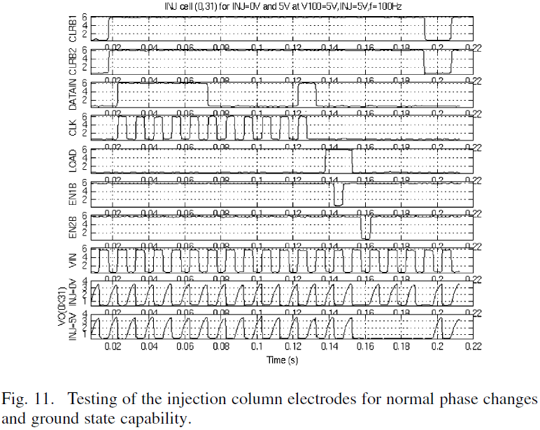
 The injection column electronics are tested by monitoring the output of a COL31 electrode site during a 180 –0 phase programming sequence and also a ground state programming sequence. During normal operation of the COL31 cell, the output should be a square wave with phase designated by the phase data bit. During injection mode, however, the cell should produce a near ground voltage for the entire time the COLINJ driver is activated. In this experiment, the cell at (0, 31) is programmed with a logic high D data and then reset when INJ is logic low and when INJ is logic high. When INJ is logic low, the electrode output will change phases in the normal fashion. However, when INJ is logic high, the ground state overrides the phase data and drives the output towards ground.
The timing diagram for the third-state electronics is shown in Fig. 11. At t=0.018 s, CLRB1 and CLRB2 are disabled. Between t=0.023 s and t=0.133 s, the address for cell (0, 31) and a logic high phase data are loaded into the shift register. At t=0.138 s, the LOAD signal is activated, at t=0.143 s, the EN1B is activated and at t=0.158 s, EN2B is activated. When EN2B is activated and INJ = 0 V, the output of cell (0, 31) changes from 180 in-phase to 0 in-phase as shown in the second to last plot in Fig. 11. However, when EN2B is activated and INJ = 5 V, the output of cell (0, 31) changes from 180 in-phase to a near ground state as shown in the last plot in Fig. 11. At time t=0.193 s, the system is reset by CLRB1 and CLRB2 and the 180 phase output state is restored. This experiment successfully demonstrates the injection column cell’s ability to realize phase changes and a ground state at the output, verifying the operation of the third-state electronics.
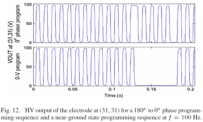
 Several HV tests are performed here to verify the 100-V output swing of the driver cell. The driver cell at (31, 31) operating with a VHH = 100 V is programmed to change phases from a 180 phase to a 0 phase square-wave output at f = 100 Hz as shown in Fig. 12, [7]. The electrode output exhibits the expected phase change behavior and shows an output voltage swing of about 100 V as directed by the performance specifications. The same driver site is also programmed to change from a 180 phase square-wave output at f = 100 Hz to a near-ground state at VHH = 100 V as shown in Fig. 12. The driver cell has been tested for a 100 V swing capability up to 200 Hz.
 Fluid droplet manipulation by the prototype PFP electrode exciter chip is now demonstrated. In the test, a droplet composed of 180 nL of PBS (phosphate buffered saline) with 700-um diameter is placed in a suspending medium of 1-bromododecane and moved across the surface of the prototype PFP electrode exciter chip coated with ~5 um of SU-8 topped with a monolayer of FluoroPel 1604 containing micro vinyl granules ~4 um across. Droplets less than 100 um in diameter, the electrode width, and droplets greater than 800 um have been used in experiments to verify droplet control. The droplet size in this experiment illustrates that droplets covering multiple electrodes are easily controlled, and otherwise has no special meaning.
The movement of the droplet within the electrode array is controlled through the Lynntech, Inc., interface board by specifying electrode addresses. In this example, the prototype PFP electrode exciter chip is operated at a HV supply of VHH = 25 V at a frequency of f = 19 Hz. “Setting” an electrode means to set its phase to the counter-phase of the surrounding electrodes and “resetting” an electrode means to set its phase to the same phase as the surrounding ones. The control sequence of the droplet is performed in four steps:
1) set the current electrode to secure the droplet;
2) reset the current electrode to release the droplet;
3) set the next electrode to move the droplet between current and next electrode;
4) reset the next electrode to center up the droplet on next electrode;
5) repeat process as desired.
Shown in Fig. 13 [7] are selected frames from a video recording a 180-nL 700-um diameter droplet of saline moving across the exciter chip’s coated top surface. The chip’s array of electrodes and electronic cells are seen in the photos. The electronic cells are 200-um^2 , with a 200-um pitch in both directions in the array. The metal3 electrodes are 100 um^2 with a 200-um pitch. The starting droplet position is marked with a pair of axes that represent the origin in each photo. In the photo labeled t = 0 s, the droplet is at the (x,y) coordinate (0, 0). In the video, the droplet moves rapidly to each new location and waits there for its next command. Images selected at the time point shown are for documenting droplet location. The droplet moves to (x,y) coordinates (0, -1), (2, -1), (2, 2), and (1, 2) as indicated on the images. Thus, droplet movement in all four directions is illustrated. Detailed characterization of the relationships among electrode size, electrode shape, electrode excitation voltage and frequency, and the various cells and chemicals [1], [4]–[6], [11]–[13] that may be of interest is beyond the scope of this paper.
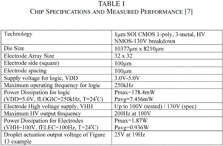
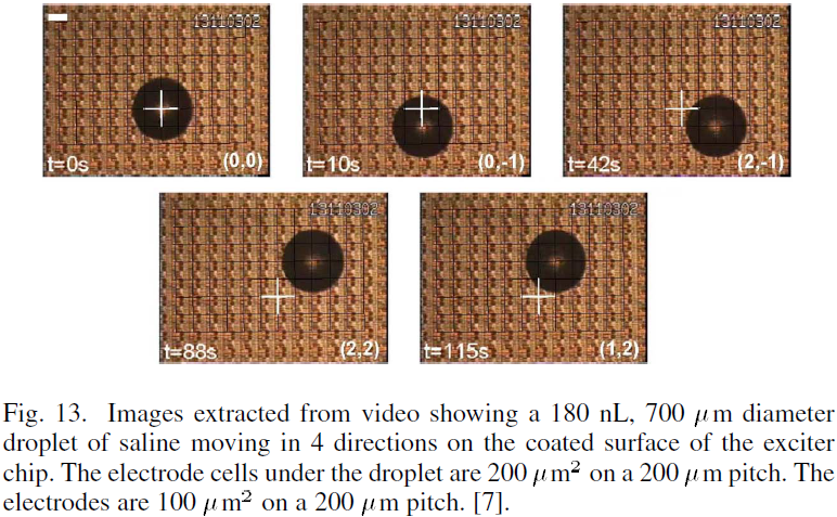 Table I [7] shows the specifications and measured performance of the prototype PFP electrode exciter chip.
VI. Summary and Conclusions
A VLSI electrode exciter chip that serves as the engine, generates the electrode excitations, for a prototype PFP has been demonstrated to precisely control the movement of droplets across its surface. This 10377 um x 8210 um 32 x 32 demonstration chip is fabricated in a commercial HV 1-um SOI CMOS technology specified for 130-V operation, and thus may be inexpensively mass-produced.
Detection of droplet location and evaluation of droplet characteristics are presently done optically off-chip. On-chip electronic droplet location detection and electronic evaluation of droplet characteristics are under development. Techniques under consideration include use of photodiodes and read out circuitry imbedded within each cell to detect the difference in received light that could indicated whether or not something is sitting on top of that cell. Also, popular [2], [3], [9]–[11] and under consideration for use is capacitive effects to detect the presense or absence of a droplet over an electrode. The analog electrode driver circuit described above could be reconfigured into a sense amp and used to detect the difference between the charge stored in a dummy cell and that present at the electrode under examination, similar to that done with commercial dynamic memory. Also, the impedance seen between a source cell and a target cell can be used to determine whether or not a droplet is present, and even used to characterize and identify the droplet within the cell [6].
Acknowledgment
The authors are grateful for the support of Department of Molecular Pathology, University of Texas, MD Anderson Cancer Center. The authors gratefully acknowledge contributions to this research by H. Lam, A.Wong, and P. Krulevitch.
References
[1] P. Gascoyne, J. Vykoukal, J. Schwartz, T. Anderson, D. Vykoukal, K. W. Current, C. McConaghy, F. Becker, and C. Andrews, “Dielectrophoresis-based programmable fluidic processors,” Lab on a Chip, vol. 4, pp. 299–309, 2004.
[2] N. Manaresi, A. Romani, G. Medoro, L. Altomare, A. Leonardi, M. Tartagni, and R. Guerrieri, “A CMOS chip for individual cell manipulation and detection,” IEEE J. Solid-State Circuits, vol. 38, no. 12, pp. 2297–2305, Dec. 2003.
[3] J. R. Keilman, G. A. Jullien, and K. V. I. S. Kaler, “A SoC bio-analysis platform for real-time biological cell analysis-on-a-chip,” in Proc. IEEE 3rd Int. Workshop System-on-Chip for Real-Time Appl., 2003, pp. 362–368.
[4] Y. Li and K. V. I. S. Kaler, “DEP based cell separation utilizing planar microelectrode array,” in Proc. IEEE 2002 Ann. Rep. Conf. Electr. Insul. Dielectric Phenom., 2002, pp. 680–684.
[5] J. Vykoukal, J. Schwartz, F. Becker, and P. Gascoyne, “A programmable dielectrophoretic fluid processor for droplet-based chemistry,” Proc. Micro Total Anal. Syst., pp. 72–74, 2001.
[6] P. Gascoyne, X. Wang, Y. Huang, and F. Becker, “Dielectrophoretic separation of cancer cells from blood,” IEEE Trans. Indust. Appl., vol. 33, no. 3, pp. 670–678, May–Jun. 1997.
[7] K. W. Current, K. Yuk, C. McConaghy, P. Gascoyne, J. Schwartz, J. Vykoukal, and C. Andrews, “A high-voltage CMOS VLSI programmable fluidic processor chip,” in Proc. 2005 VLSI Circuits Symp., Jun. 2005, pp. 72–75.
[8] K. W. Current, K. Yuk, C. McConaghy, P. Gascoyne, J. Schwartz, J. Vykoukal, and C. Andrews, “A high-voltage integrated circuit engine for a dielectrophoresis-based programmable microfluidic processor,” in Proc. Int. Conf. MEMS, Nano, Smart Syst., Jul. 2005, pp. 153–158.
[9] A. Enteshari, G. A. Jullien, O. Yadid-Pecht, and K. V. I. S. Kaler, “All CMOS low power platform for dielectrophoresis bio-analysis,” in Proc. 31st Eur. Solid-State Circuits Conf., 2005, pp. 339–342.
[10] A. Romani, N. Manaresi, L. Marzocchi, G. Medoro, A. Leonardi, L. Altomare, M. Tartagni, and R. Guerrieri, “Capacitive sensor array for localization of bioparticles in CMOS lab-on-a-chip,” in Proc. IEEE Int. Solid-State Circuits Conf. Dig. Techn. Papers , Feb. 2004, pp. 224–225.
[11] E. J. Griffith, S. Akella, and M. K. Goldberg, “Performance characterization of a reconfigurable planar-array digital microfluidic system,” IEEE Trans. Computer-Aided Des. Integr. Circuits Syst., vol. 25, no. 2, pp. 345–357, Feb. 2006.
[12] J. A. Schwartz, J. V. Vykoukal, and P. R. C. Gascoyne, “Droplet-based chemistry on a programmable microchip,” Lab on a Chip, vol. 4, pp. 11–17, 2004.
[13] J. A. Schwartz, “Dielectrophoretic Approaches to Sample Preparation and Analysis,” Ph.D. Dissertation, Dept. Molec. Pathol., Univ. Texas, Austin, Dec. 2001.