

 0
0
 0
0
By Claudia Wong, Kelvin Yuk, G. R. Branner and Syed Reza Bahadur
Originally Appears: European Microwave Circuits Conference, pp. 587-590, Oct. 2011.
Abstract
A wideband frequency doubler based on AlGaN/GaN HEMT devices is presented. Rationale for the use of filters to improve the bandwidth performance of a frequency doubler is described. Input and output networks consisting of a harmonic reflector and bandpass filter are designed to provide adequate bandwidth response and high power with small conversion gain. A demonstration circuit achieves 13.2% fractional bandwidth at fo= 3.33 GHz with a maximum output power at 30.2 dBm.
I. Introduction
Frequency multipliers are an essential part of microwave communication systems. In systems requiring several, coherent reference signals, signal source generation from multiple oscillators can be expensive to implement. Frequency multipliers provide an affordable means to convert a single low noise, low distortion source to a variety of systems as part of a signal distribution scheme. Any nonlinear component can be designed to generate harmonics, but active frequency multipliers using transistors have the important benefit of low conversion loss over passive multipliers using diodes or varactors. However, due to the nonlinear properties of active frequency multipliers and the complexity with which they operate, design of these circuits is non-trivial. The creation of high power AlGaN/GaN (GaN) HEMTbased frequency multipliers established a new application for III-V semiconductor devices [1][2]. Recent work in this area has led to gain and power levels not previously seen in microwave frequency multiplier design. Design using GaN HEMTs lends the possibility of delivering large amounts of power to systems consisting of many subsystems or arrayed configurations. Some of the techniques used to design frequency doublers and triplers involve the use of harmonic manipulation by load-/source-pull analysis [1][2]. This approach allows for a direct and precise synthesis of harmonic termination networks and has resulted in exceptional results for narrowband multipliers. However, it is often difficult to achieve wide bandwidth frequency multiplication with these narrowband synthesis methods. In this work, a wide bandwidth frequency doubler based on the Cree CGH40010 GaN HEMT [3] transistor is designed using filtering techniques. The frequency multiplier topology and performance criteria are described in Section II. Section III describes some important aspects of the device model. Section IV explores the rationale for broadbanding using filtering concepts. Section V describes the design of the broadband prototype circuit developed here. Section VI presents the measured performance of the doubler and Section VII concludes this work.
II. Frequency Multiplier Topology and Performance Criteria
The topology of the frequency multiplier presented here is shown in Fig. 1 and consists of a single GaN HEMT transistor, cascaded with performance-enhancing passive networks at the input (M1) and output (M2). The single-transistor, singleended topology is advantageous in that it allows for straightforward design of low-loss microstrip networks and alleviates the problems associated with device mismatch.

Figure 1. Network topology for the high-power, single-ended frequency multiplier
The active device used in this frequency doubler is the commercially available CGH40010 10W GaN HEMT manufactured by Cree, Inc. The software used in this work is Agilent Advanced Design Software (ADS). Some of the main performance criteria for the frequency doubler are the second harmonic output power (Pout2), conversion gain CG2 and fractional bandwidth FBW.
III. Active Device Modeling
High-accuracy CAD-based design approaches provide an accurate means of predicting the harmonic generation from frequency multipliers. Fortunately, a precise model is available for the device under investigation [4]. The schematic for the device model is shown in Fig. 2.

Figure 2. Nonlinear device model of the GaN HEMT
IV. Design for Wideband High Power Frequency Performance
A perusal of the published literature on active microwave frequency multipliers will reveal that the vast majority of these developments produce relatively narrowband performance. This results in multiplied conversion gain or power output typically in the vicinity of 5% bandwidth [4]. Several results have been obtained employing a technique which utilizes a bandpass structure as part of the output network (M2) in Fig. 1 to simply filter the desired harmonic and suppress unwanted frequencies while others have employed the same technique to obtain a widened bandwidth performance. However, an examination of the underlying science of this technique has, to the best of the authors’ knowledge, not been forthcoming.
In the following discussion, a theory will be advanced to explain why this technique provides widened bandwidth, improved gain, and power at the prescribed harmonic utilizing a prescribed design technique.
It should be understood that the broadbanding with significantly increased gain is not simply the outcome of two networks together in cascade, one of which is band-limiting. The discussion will utilize the network topology shown in Fig.1 where the active device is embedded between input and output embedding networks M1 and M2. The attention will be primarily focused on M2.
Utilizing a fundamental device model derived from measured device data, the discussion will be based on a three stage exposition, providing quantitative results in each case.
The first case is just the active device alone with M2 (and M1) straight through lines terminated in 50Ω. The second case demonstrates the results achieved utilizing a fundamental reflector network for M2 while the third case discusses the broadbanding effect with gain utilizing a bandpass structure. The center frequency for the demonstration is 3.00 GHz centered in the 2-4 GHz band.
A. Technique for Producing Frequency Conversion Performance Given a Prescribed Active Device
The design of an active frequency multiplier is dependent on gate and drain bias levels, input power level, and the performance of input (M1) and output (M2) networks as shown in Fig. 1. An in-depth discussion of methods of active frequency multiplier design can be found in [5]-[6]. Although wideband lower power active frequency multipliers have been developed in the past, no detailed theory justifying the approach has, to the author’s knowledge, been advanced aside from the balanced active multiplier approach provides higher output power due to the ability of the additional swing due to differential operation. Numerous typical realizations in the past have been based on load pull techniques or a straight forward inclusion of a bandpass filter in M2 with center frequency at the desired harmonic.
B. Broadband Design Rationale
1) Examination of the Design Rationale Based on Principle Nonlinearities
A perusal of the general GaN model presented above in Section III will reveal the existence of seven principal nonlinearities capable of producing harmonic generation (the nonlinear drain conductor as usual, does not appear in the model circuit diagram). To obtain an understanding of the fundamental multiplication mechanism across a wide band of frequencies, the discussion in this section is focused on three primary harmonic generation mechanisms as shown in Fig. 2. These are the controlled current source Ids, the gate diode Dgs, and gds, the drain-source conductance. While this analysis and discussion has to be extended to include other device nonlinearities and parasitics for the practical realizable design case (and the outcome of this will be presented in Section V below), just the three nonlinearities identified above provide sufficient information to understand the basic mechanism for wideband high power performance.
The model shown in Fig. 3a has been implemented in the ADS software. To provide realism for the actual GaN device, this model has been extracted by using the actual measured CREE CGH40010 HEMT nonlinear data for measured pulsed IV characteristics as shown in Fig. 3b.
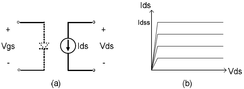
Figure 3. (a) Schematic and (b) IV characteristics of idealized model for principle nonlinear analysis

Figure 4. Simulated harmonic output of ideal model
This model, properly biased (at pinchoff) for optimal even harmonic generation in a 50Ω system, has been simulated in ADS as shown in Fig. 4. These plots demonstrate the output power produced by the GaN model of Fig. 3a at fo, and Fig. 3b at 2fo. Based on the realistic, practical model of Section III, the bias values were chosen to be -2.8 V and 28V at the gate and drain respectively, while the input power level was +30 dBm. Note from Fig. 4, that under the above conditions the output powers are constant over frequency at 40 and 12.5 dBm respectively for at fo and 2fo. This is to be expected due to the simplistic model having no frequency dependent parasitics. These power values are constant over an fo frequency band of 2 to 4 GHz (4 to 8 GHz 2fo band).
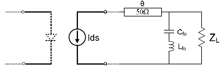
Figure 5. Simple LC resonator network connected to the output of the ideal transistor model (DC network not shown)
Of the several approaches that have been used to explain active device frequency multiplication, one contends that increased harmonic power output may be achieved by reflecting the fo power emerging from the drain back into the drain at the correct phase angle for proper mixing due to the presence of the nonlinear conductance. This can and is frequently achieved using a simple LC resonator or “reflector” network as illustrated in Fig. 5.
Fig. 6 shows the new response of the active multiplier circuit which employs the single reflector network of Fig. 5 in the output network M2. Observe that for the identical input power and biases, the 2fo output power has now been increased by 26.3 dB to a value of 38.83 dBm. Note that the fo output power has been significantly decreased. These improvements are narrowband as was conjectured earlier. An explanation for the 26.3 dB improvement in 2fo output power is that the fo signal has now been reflected back and mixed in the nonlinearity of the drain-source conductance. Fig.7 is a separate plot of the S11 and S21 responses of the passive output network M2 alone. Fig.7a is a plot of |S11| (dB) for M2 due to the action of the reflector network (Fig.5). This response essentially becomes equal to unity at fo, thus indicating that all the power at fo is essentially being reflected back into the drain. Note also that this same response of Fig.7a begins to decrease from |S11| = 1 as the frequency moves off the resonance value. Thus, the amount of 2fo created as a result of reflected fo power also begins to decrease. In order to broadband the amount of 2fo output power based on the above explanation, therefore, it is necessary to wideband the reflection coefficient of the M2 network.
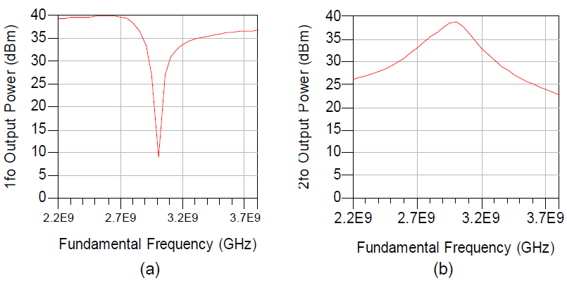
Figure 6. Simple L-shaped resonator network connected to the output of the ideal transistor model (DC network not shown)

Figure 7. Selected S-Parameter Response of Output Network M2 with Reflector Network
2) Method to Obtain Broadband Performance
As shown in Fig. 5, the tuned LC network in the M2 network is now replaced with a 3-pole maximally flat 33.3% bandpass filter (BPF) structure centered at 2fo=6.00 GHz. As previously explained, the BPF filter is preceded with the same length of transmission line to provide optimal phasing. A plot of the revised response of the S11 and S21 of this new output network M2 is shown in Fig. 8. In the figure, this new M2 network has the expected S21 performance of the 33.3% BPF (Fig.8b). Also, it is observed that now the reflection coefficient is essentially unity across the entire 2 to 4 GHz range, inferring that any in band fo output power will be essentially returned back into the drain of the active device.
Finally, Fig. 9 is a plot of the response of the frequency doubler incorporating the new M2 network in Fig.8. Here it is observed that using ideal M2 network elements that the fo response is now decreased to less than 20 dBm across the 2 to 4 GHz band as contrasted with previous results of 40 dB (Fig.9a). Furthermore, it may be seen that the 2fo output power now represents a bandwidth of some 33.3% as compared with the previous narrowband results.
The preceding discussion has provided the explanation why, by proper choice of transmission line (TL) length, increased grain and bandwidth may be obtained utilizing a TL/BPF cascaded structure for M2.
To employ this theory in a practical design case, the actual device with all its parasitics must be considered as shown in Fig.2.

Figure 8. Selected S-Parameter Response of Revised Output Network M2 with BPF

Figure 9. Frequency Doubler Response with new M2 network
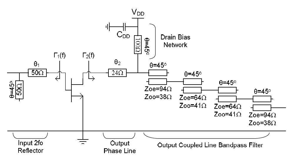
V. Wideband High Power Frequency Multiplier Design
The self-heating, charge trapping effects and parasitics of the HEMT device necessitate a more complex device model for practical design. The precision wideband model for the CREE CGH40010 GaN HEMT has been previously developed in our laboratory [4] and is employed for the design of the wideband high power frequency doubler described below.

Figure 10. Network topology for the high-power, single-ended frequency multiplier
This frequency doubler is to operate at an input frequency of 3.33 GHz (2fo = 6.66 GHz), 1W 2fo in band output power, and at least a 13% bandwidth.
The design philosophy and multiplier system configuration is based on the structure of Fig. 1. On the gate of the device is the input network M1 which consists of an offset 2fo O.C. stub reflector.
The output network M2 in Fig. 1 is developed as described in the preceding section. It consists of a length of transmission line in cascade with a bandpass filter. The length of Zo = 24Ω microstrip line precedes the filter.
As explained in the previous section, the primary purpose of this phase line is to provide an optimal phase offset for the band rejected frequencies for reflection back to the drain of the device to produce additional 2fo output power, and to provide for additional drain parasitics of the GaN transistor that were previously unaccounted by theory.
The filter used in M2 is a 3-pole maximally flat 20% bandwidth coupled line bandpass filter centered around 2fo = 6.66 GHz. Because the filter has been synthesized as a coupled line bandpass structure, a special bias network has been developed as shown in Fig.10.
VI. Analysis of Results
Fig.11 shows the 2fo output power with respect to the fundamental input frequency. A 13.2% 3-dB bandwidth has been achieved. A maximum 30.2 dBm (~1W) of 2fo output power has been achieved for Pavs = 30 dBm. 2fo output power has been closely predicted over a band of frequencies. The maximum conversion gain is 0.2 dB and maximum drain efficiency (Eta) is 4.8%, shown in Fig. 12a and 12b, respectively. To the authors’ knowledge this is the first reported high power broadband frequency doubler. Previous works in high power frequency doublers have yielded 4% bandwidth [1].
Fig. 13 shows the fo, 2fo, and 3fo output power for Pavs = 19-36 dBm. The output power is also closely predicted at each harmonic for varying input power levels.
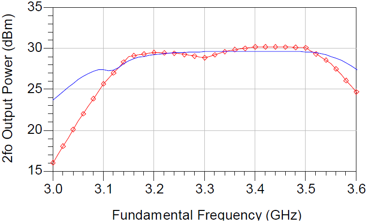
Figure 11. Measured (Dotted) and Simulated (Solid 2fo Output Power (dBm) vs. fo Input Frequency (GHz) of Wideband Frequency Doubler
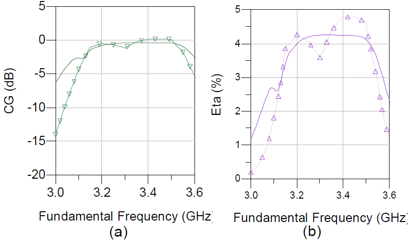
Figure 12. Measured (Dotted) and Simulated (Solid) 2fo Conversion Gain (dB) vs. Fundamental Frequency (GHz) (a), 2fo Eta (%) vs. Fundamental Frequency (GHz) (b).
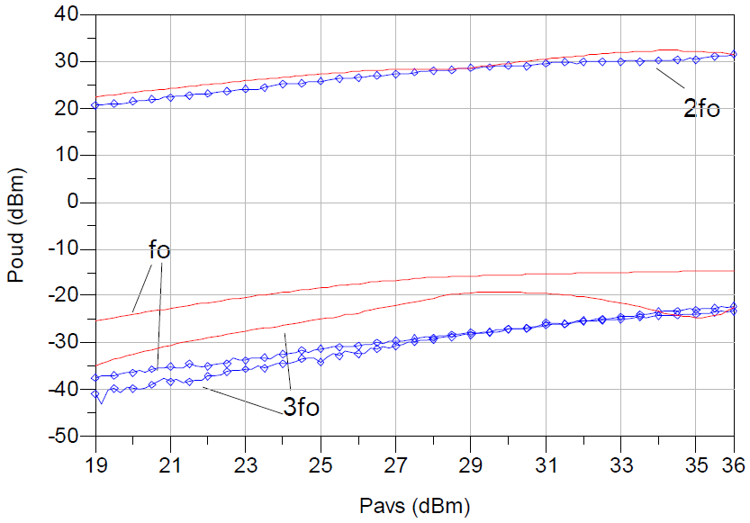
Figure 13. Measured (Dotted) and Simulated (Solid) fo, 2fo, 3fo Output Power (dBm) vs. Pavs (dBm) at f = 3.33 GHz
VII. Conclusion
This paper has presented theory and techniques leading to development of high power AlGaN/GaN HEMT wideband active frequency multipliers.
A wideband high power active doubler with a maximum 2fo output power of 30.2 dBm (~1W), bandwidth of 13.2%, a maximum conversion gain of 0.2 dB, and a maximum drain efficiency of 4.8% has been realized.
This broadband frequency doubler was developed using a highly accurate GaN HEMT model [4] and incorporates a side coupled bandpass filter realization as a fundamental constituent.
Acknowledgment
The authors would like to acknowledge Dr. Wayne Martin for his generous contributions in support of this work.
References
[1] K. Yuk, G. R. Branner, C. Wong, “High Power, High Conversion Gain Frequency Doublers using SiC MESFETs and AlGaN/GaN HEMTs,” 2010 IEEE MTT-S International, Microwave Symposium Digets (MTT), 2010, pp. 1008-1011.
[2] K. Yuk, C. Wong, G. R. Branner, “Design of a High Power X-Band Frequency Tripler Using a AlGaN/GaN HEMT Device,” Microwave Conference (EuMC), 2010 European, 2010, pp. 612-615.
[3] “CGH40010 10W, RF Power GaN HEMT datasheet Rev. 1.3 – March 2007,” Cree, Inc., Durham, NC, 2007. [Online]. Available: http://www.cree.com/products/pdf/CGH40010.pdf.
[4] K. Yuk, G.R. Branner, D. McQuate, “An Improved Empirical Large-Signal Model for High-Power GaN HEMTs Including Self-Heating and Charge-Trapping Effects,” IEEE Trans. on Microwave and Theory Tech., vol. 57, no. 12, pp. 756-756.
[5] D. G. Thomas, G.R. Branner, B. P. Kumar, “Microwave and Radio Frequency Mutlipliers,” Encyclopedia of RF and Microwave Engineering, vol. 3, Wiley Interscience, 2005, pp. 2663-2703.
[6] J. Johnson, “Theory and Design of Active Frequency Multipliers,” PhD Disseration, University of California, Davis, 2004.
[7] Y. Chung, K. M. K. H. Leong, and T. Itoh, “AlGaN/GaN HEMT X-band frequency doublers with novel fundamental frequency reflector scheme,” IEICE Trans. Electron., vol. E86-C, no. 8, pp. 1416-1421, 2003.
[8] D. Barataud, C. Arnaud, B. Thibaud, et. al., “Measurements of Time-Domain Voltage/Current waveforms at RF and Microwave Frequencies Based on the Use of a Vector Network Analyzer for the Characterization of Nonlinear Devices—Application to High-Efficiency Power Amplifiers and Frequency-Multipliers Optimization,” IEEE Trans. Instr. and Meas., vol. 47, no. 5, pp. 1259-1264, October 1998.
[9] Y. Chung, D. Ahn, and T. Itoh, “Alternating Input Power Dividing Technique for High Conversion Gain Frequency Doubler,” Euro. Microw. Conf., vol. 2, pp. 491-493, Oct. 2003.