

 0
0
 0
0
By Kelvin Yuk, G.R. Branner
Originally appears: IEEE Transactions on Microwave Theory and Techniques, Volume 56, Issue 11, Part 2, pp.2671 – 2680, Nov. 2008.
An empirical large-signal model for high power microwave SiC MESFETs capable of predicting self-heating thermal behavior is presented. A generalized drain current equation based on pulsed-gate IV characteristics measuring up to 2A and 58V is presented along with its dependence on temperature. A thermal subcircuit with a nonlinear thermal resistance characterized by a dc method is used to model the temperature behavior of the device. The effect of substrate trapping is modeled as a gate-source voltage correction. The complete drain current model accurately predicts pulsed-gate and pulsed-gate-and-drain IV characteristics for various quiescent biases as well as static IV characteristics. The complete large-signal model is shown to accurately predict S-parameters, large-signal output and input reflected power across biases and frequencies, and third-order intermodulation products.
I. Introduction
Research in silicon carbide microwave devices and circuits has been growing rapidly. Devices such as SiC MESFETs are becoming a viable solution to the growing demands of robust, high power microwave applications and have become increasingly competitive with other high power technologies like GaN. Some of the advantages of SiC MESFETs are its high power density and high drain-source breakdown voltage making it ideal for high power applications.
The typical application for SiC MESFETs is in high power narrowband and broadband amplifiers. A number of SiC MESFET amplifiers have been demonstrated [1] and SiC MESFET amplifiers generating greater than 30W at high frequencies have been reported [2]. Other circuits which have been developed using SiC MESFETs include mixers and oscillators [3],[4] and this demonstrates the potential to combine high gain and power output with signal processing functionality. Design of such circuits requires the availability of an accurate large-signal active device model.
Some recent empirical large-signal SiC MESFET models based on the work of Angelov [5-7] have been reported in [8-12]. The model in [8] has shown excellent drain current and capacitance modeling results. It has also been shown to accurately predict the large-signal power output of a specific amplifier implementation. Also, models presented in [9-11] accurately predict small-signal performance and power output for lower power GaN and SiC MESFET devices by using a modified Chalmer’s model. The work in [12] has demonstrated accurate modeling of both output and input reflected harmonic power for three harmonics by using a simple topology and a single drain current model based on pulsed-gate-and-drain IV characteristics.
One of the challenges in developing a large-signal SiC MESFET model valid over various biases is modeling the self-heating which arises from the high power nature of the device. Numerous studies have been performed to characterize and model bias-dependent thermal effects by using dynamic IV measurements [13]-[18]. Some of the techniques have employed the integration of static biases into drain current models [13-16] while others have characterized thermal behavior of the device [17] and applied changes in temperature directly to circuit model parameters based on dissipated power [9-11,18]. In this work we employ a combination of these techniques to develop a model that utilizes a well defined thermal model and trapping correction that accurately predicts pulsed, DC and RF characteristics over various quiescent biases. It is the writers’ opinion that none of the previous work stated has demonstrated such modeling performance over the high voltage, high current and high power ranges as that presented in this work. The integration of dispersion effects in the model is vital in predicting the large-signal behavior of SiC MESFETs.
The current paper presents an empirical large-signal model utilizing the Cree CRF-24010 10W Silicon Carbide MESFET [19]. The unmatched SiC MESFET is packaged in a 440166 package with flange and measures about 14.09mm x 4.19mm x 3.43mm with a junction to case thermal resistance of 5.6 C/W [19]. A large-signal model for this device is also available from the manufacturer [20], but little technical information about it is known other than it is based on a modified Curtice-cubic model [21]. The model presented in this paper can accurately predict pulsed-gate, pulsed-gate-and-drain and static IV characteristics over a large range of biases by employing a self-heating thermal model and gate-voltage correction that accounts for trapping. The model is also shown to predict the small-signal and large-signal output and input reflected RF behavior over different biases. The model can also predict RF output and input reflected power over a moderate frequency band as well as third-order intermodulation products under large-signal drive.
In Section II, the large-signal model is presented. A generalized drain current model is described and implemented into a simple large-signal model topology. The thermal model predicting changes in the SiC MESFET junction temperature and its effect on the drain current is described. The gate-source voltage correction accounting for dispersion due to substrate trapping is presented. The complete model including nonlinear current source, small-signal parasitics, nonlinear capacitances, junction diodes and thermal circuit is implemented in the Agilent ADS software package. In Section III, the fidelity of the model is verified by comparing measured and modeled pulsed-gate and pulsed-gate-and-drain IV characteristics under various quiescent bias conditions as well as static IV characteristics. The performance of the model is also verified by comparing model predictions against measured small-signal S-parameters, large-signal harmonics for various biases and against frequency, and third-order intermodulation products. Conclusions are given in Section IV.
II. Model Description
The large-signal model with included thermal subcircuit is shown in Fig. 1.
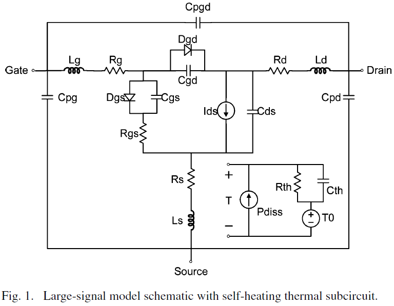
In all measurements presented here, the SiC MESFET was mounted on an aluminum plate fastened to a heat sink and cooling fan for temperature reduction. The model is seen to be composed of package parasitics and nonlinear elements: Ids, the drain-source current, Dgs, the gate-source diode, Dgd, the gate-drain diode, Cgs, the gate-source capacitance, Cgd, the gate-drain capacitance and Cds, the drain-source capacitance.
A. Large-Signal Drain Current Modeling
Although, the original Chalmers drain-current model [5] assumes separability of Vgs and Vds terms and straight linear dependencies on Vds, more recent work by the same group has shown a strong interdependence of Ids parameters on both Vgs and Vds. This appears necessary to accurately model high power devices that exhibit significant self-heating and current dispersion [9-11].
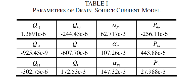
In devices such as high power SiC MESFETs, it is especially important to model the nonlinear relationships between Ids and Vgs across the entire range of Vds in both saturation and linear regimes. Such an expansive fit requires functions of adequate generality which can be tailored for the particular device of interest. The drain current model employed in this work is presented in (1) and is a variation of the Chalmers model [5-7].
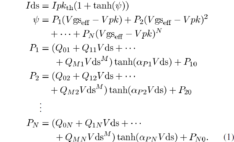
Here, the Pn parameters of the power series describing the Vgs dependence are each a power series expansion of Vds multiplied by a tanh(αVds) term and shifted by Pno, the bias independent term of Pn. The parameter Vpk is normally the Vgs value at the peak transconductance, gmpk. Although gmpk can vary with Vds in HEMT devices [5], this variation is not strong in SiC MESFETs except in the low Vds regime and is accounted for by the use of the Pno and tanh(αPnVds) terms for each Pn parameter.
Since the SiC MESFET does not present a bell-shaped transconductance by the same mechanism as in HEMTs, gmpk loses its usual meaning [5]. Therefore, it is necessary to select a certain Vpk such that the drain current model can be used effectively. For the model presented here, Vpk is chosen at the maximum transconductance point found within the available IV dataset which occurs at Vgs=0.5V, the highest available gate-source bias. The dataset presented here is large and allows the selection of Vpk just below the onset of forward conduction of the gate-source diode. The subsequent Ipk values are defined by the Ids corresponding to Vpk=0.5V across the Vds bias range [12]. Although Ipk as a function of Vds can be table-based in the absence of self-heating it is modeled here using the expression
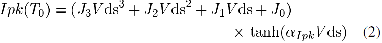
where the Jn and αIpk values are fitting parameters.
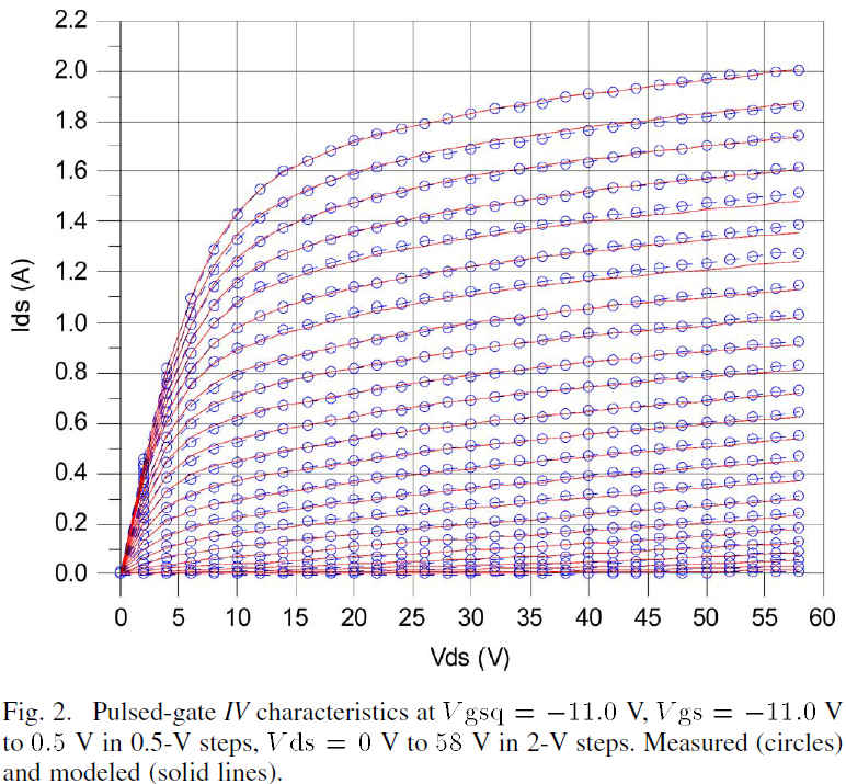
In characterizing the SiC MESFET, a multiplicity of pulsed-gate IV measurements were taken to obtain the device’s performance in the absence of any static self-heating conditions. The IV characteristics of the device were measured from Vgs=-11.0V to 0.5V in 0.5V steps and Vds=0V to 58V in 2V steps with a quiescent gate bias of Vgsq=-11.0V using a pulse width of 100ns and pulse period of 400ms. The pulse parameters are carefully chosen here to prevent the onset of dispersion during the pulsed state and sufficient relaxation of the dynamic device behavior between pulses [22].
The modeled versus measured pulsed-gate IV values are shown in Fig. 2. These computed results show that for a large range of biases the formulation is extremely effective at modeling the pulsed-gate IV characteristics with zero static power dissipation. The parameters used to realize the model are presented in Table I. All other Qnm and Pno parameters are equal to zero.
B. Thermal Modeling and the Effect on Drain Current
It is important to consider the thermal behavior of the device when developing a generalized model since the quiescent bias point will substantially affect its performance. The equivalent circuit model for the thermal behavior of the device was shown previously in Fig. 1 [8]. This circuit approximates the temperature and thermal charging and discharging of the device according to the expression
![]()
where T is the temperature, T0 is the ambient temperature, is the change in temperature and is the thermal time constant.
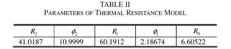
There exist a number of approaches for extracting the nonlinear thermal resistance Rth, which relates the junction temperature to the dissipated power [23]-[28]. In the approach used here, Rth was extracted from DC forward bias gate-source diode current measurements which were performed over a range of static drain-source voltages in a manner similar to that in [17,23]. The technique provides values for Rth characterized over various dissipated powers.
The thermal resistance measured up to 27W is shown in Fig. 3 and modeled by the formula
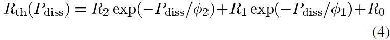
where R0 is a constant term, R1 and R2 are the coefficients of the first and second exponential terms, respectively and φ1 and φ2 are the decay constants of the first and second exponentials, respectively. The extracted model parameters are provided in Table II. The thermal resistance saturates as Pdiss increases due to the saturation of the junction temperature at around 570K.
Integration of the self-heating effects can be done primarily by modifying the Ipk equation according to the change in temperature as in [7]. Here the temperature dependent Ipkth is written as

where Ipk(T0) is Ipk with no self-heating, is the time-dependent temperature change computed by the thermal circuit and KIpk is a fitting parameter. Equation (5) is mathematically equivalent to the relationship presented in [7], but is written in this form to emphasize the fact that Ipk will generally decrease as temperature increases. A bias dependent term KIpk is used to satisfy the above equation for all quiescent biases and can take the form of a table or an analytical expression. Here, the expression used for KIpk is
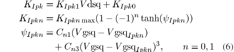
where KIpkn, KIpknmax, Cn1, Cn3 and VgsqIpkn are fitting parameters.
This thermal relationship is applied to Ipk at Vpk=0.5V for static gate biases of Vgsq=-11.0V to -3.0V in 0.5V steps from Vds=0V to 58V in 2V steps. The resulting Ipk values at these quiescent biases are shown in Fig. 4. Comparing the modeled versus measured data, it is observed that the relationship described by (6) is valid and effective for the modeling of the thermal effects on Ipk.
In addition to Ipk, the Pn parameters will also vary with temperature, though its effect on Ids as a function of self-heating is not as pronounced as that of Ipk. Pn is modified as a function of temperature using the following relationship [10]
![]()
where KPn is similar in function as KIpk described above but can be formulated using a simpler expression.
The transient change in Ids from one temperature to another will follow the same exponential temperature response described in (3). Therefore, once Rth is known, and the thermal capacitance Cth can be approximated from transient pulsed-gate Ids behavior measured over long pulse durations. A Cth value of 4.20mF was extracted from a long pulsed-gate transient measurement of Ids with a pulse width of 2ms for Vgsq=-11.0V pulsed to -3.0V at Vds=55V.
C. Dispersion Due to Trapping
Pulsed-gate IV responses can be used to characterize the thermal behavior of the SiC device using a relatively small number of IV datasets. However, pulsed-gate-and-drain IV characteristics provide a better prediction of large-signal behavior at a given operating point. To incorporate the effects of steady-state substrate trapping, a gate-source voltage correctional term is incorporated in the drain current model presented in this paper. This enables the model to accurately predict both pulsed-gate and pulsed-gate-and-drain IV characteristics.
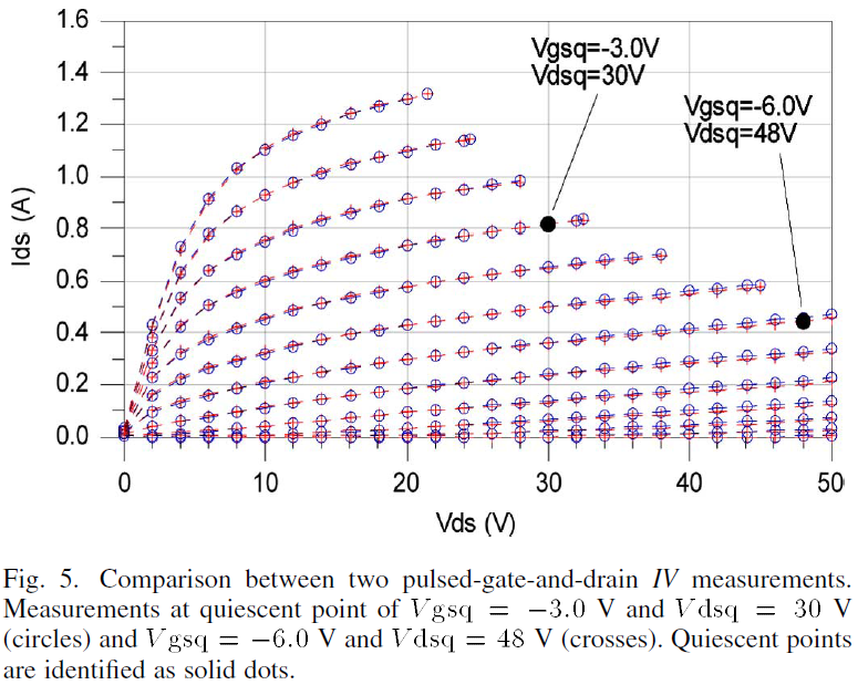
It has been shown that dispersion due to traps in SiC MESFETs is due primarily to substrate traps [29] which are the main focus here. A Nanometrics DiVA Dynamic I-V Analyzer [30] was used to measure the pulsed-gate-and-drain IV characteristics of the SiC MESFET using 200ns pulses separated by 1ms. Two sets of pulsed-gate-and-drain IV characteristics, one biased at Vgsq=-3V, Vdsq=48V and the other biased at Vgsq=-6V, Vdsq=48V are compared in Fig. 5. The device dissipates about 25W at both quiescent biases and shows very similar drain current characteristics implying that dynamic substrate trapping behavior is not present [29,31]. This means that only steady state trapping affects the drain current performance when using pulse durations of 200ns or less.
In this work, the effect of steady state trapping has already been included in the drain current model derivation based on pulsed-gate IV characteristics. Therefore, an adjustment of the effective gate-source voltage based on the pulsed and quiescent drain biases can be formulated by writing:
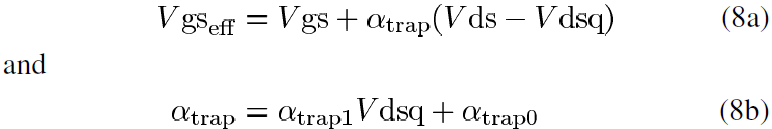
where Vgs is the instantaneous gate-source voltage, Vds is the instantaneous drain-source voltage, Vdsq is the quiescent drain-source voltage and αtrap0 and αtrap1 are fitting parameters. Equation (8a) is a modified version of that found in [31,32] in that the calculation of the backgate voltage has been bypassed for a direct computation of the substrate trapping effect on the effective gate-source voltage. Good results can be achieved by making αtrap a linear function of the quiescent drain voltage as shown in (8b).
The comparison of modeled and measured pulsed-gate-and-drain IV characteristics are provided in section III.
D. Parasitics and Capacitance Modeling
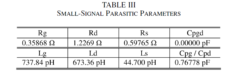
The extrinsic small-signal model parameters are extracted based on standard methods using statically biased S-parameter measurements [33,34]. The extrinsic capacitances are extracted from pinched-FET S-parameters, while the extrinsic inductances and resistances are extracted using cold-FET S-parameter measurements. The parameter values for these parasitics are provided in Table III. The intrinsic device parameters were extracted from hot-FET S-parameter measurements taken with the device biased in the active region for Vgs values ranging from -10V to -5V in 1V steps and Vds from 0V to 60V in 2V steps. The intrinsic Cgs, Cgd, Cds, gm and gds are extracted from each set of hot-FET S-parameters and placed in a full small-signal model such that there is good agreement between the measured and modeled responses. The extracted values for the voltage dependent capacitors Cgs, Cgd and Cds are then modeled using the Chalmers capacitance model and implemented into Agilent ADS in the form of charge equations [7].
E. Diode Modeling
The characteristics of the gate-source and gate-drain diodes in forward conduction are modeled using the standard diode equation. The saturation currents and thermal voltages of the diodes are extracted by measuring the device in forward conduction [35]. These forward conduction gate current measurements are also used to assist in the extraction of the parasitic gate, drain and source resistances as described by [35].
III. Experimental Model Verification
In this section, the performance of the drain current model is compared with measured pulsed-gate IV characteristics at four different quiescent gate biases, with pulsed-gate-and-drain IV characteristics at three different quiescent biases and finally with static IV characteristics. To validate the RF performance of the model, it is compared with measured S-parameter data to verify the small-signal accuracy, and measured output and input reflected power data for the first three harmonics to verify the large-signal accuracy. The RF performance of the device is measured and modeled at two different biases to exemplify the broad range of validity. Additionally, comparisons with large-signal measurements as a function of frequency and with measurements of third-order intermodulation products obtained from a two-tone test are used to validate the fidelity of the model.
A. Pulsed-Gate IV, Pulsed-Gate-and-Drain IV and Static IV Characteristics
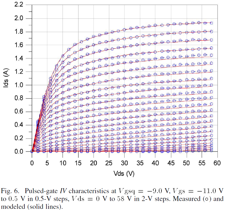
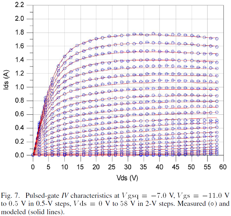
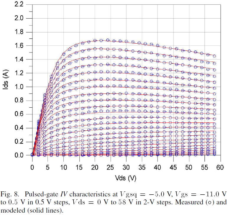
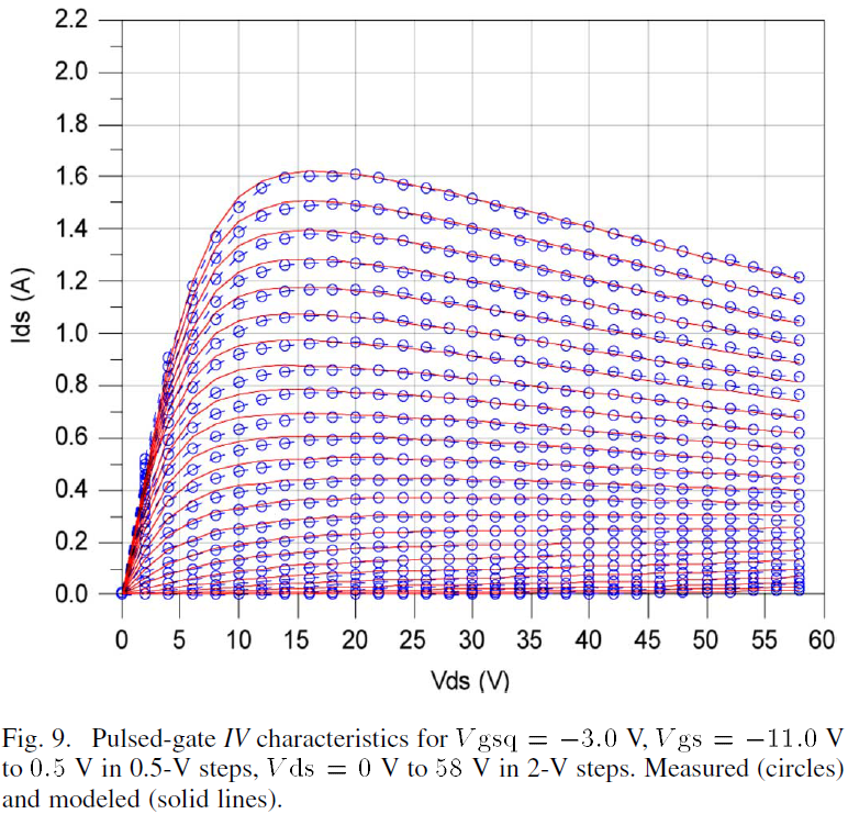
The pulsed-gate IV measurements described in Section II were conducted for quiescent gate biases from Vgsq=-11.0V to -3.0V and used for verification of the thermal model and its effect on the drain current. The pulsed behavior of the model is computed using transient simulations and the resulting pulsed-gate IV curves for Vgsq=-9.0V, -7.0V, -5.0V and -3.0V are given in Figs. 6 – 9, respectively. According to these results, the large-signal model with thermal circuit is capable of closely reproducing the pulsed-gate IV behavior. These curves serve to illustrate the efficacy of the thermal portion of the model. The model modifies the drain current at zero static power dissipation, as was shown in Fig. 2, into the respective drain current at static power dissipations defined by the quiescent bias.
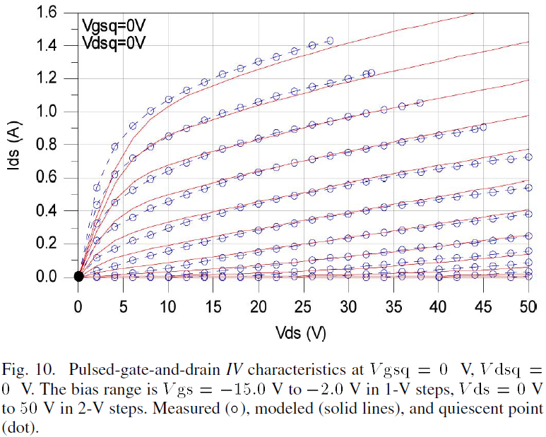
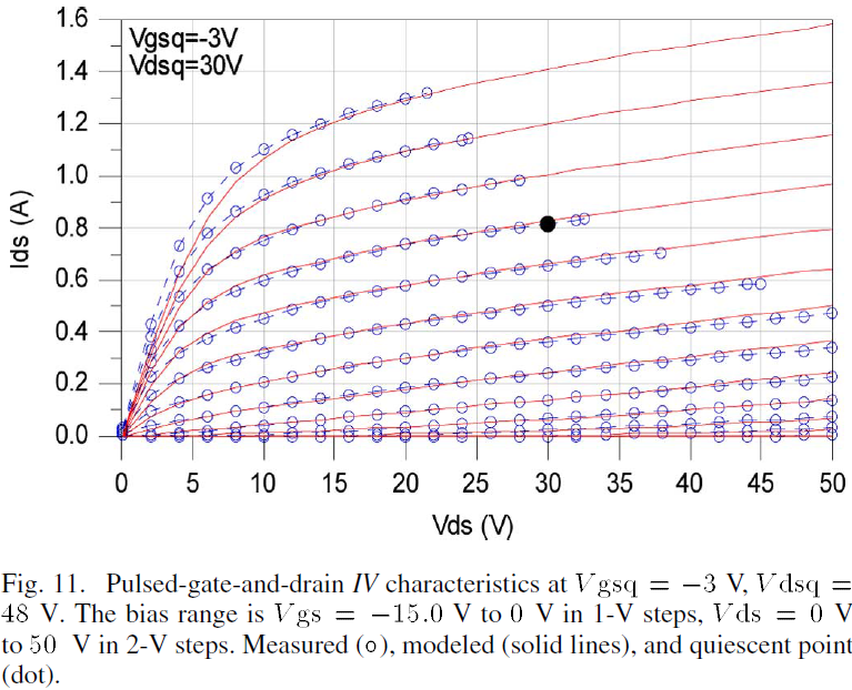
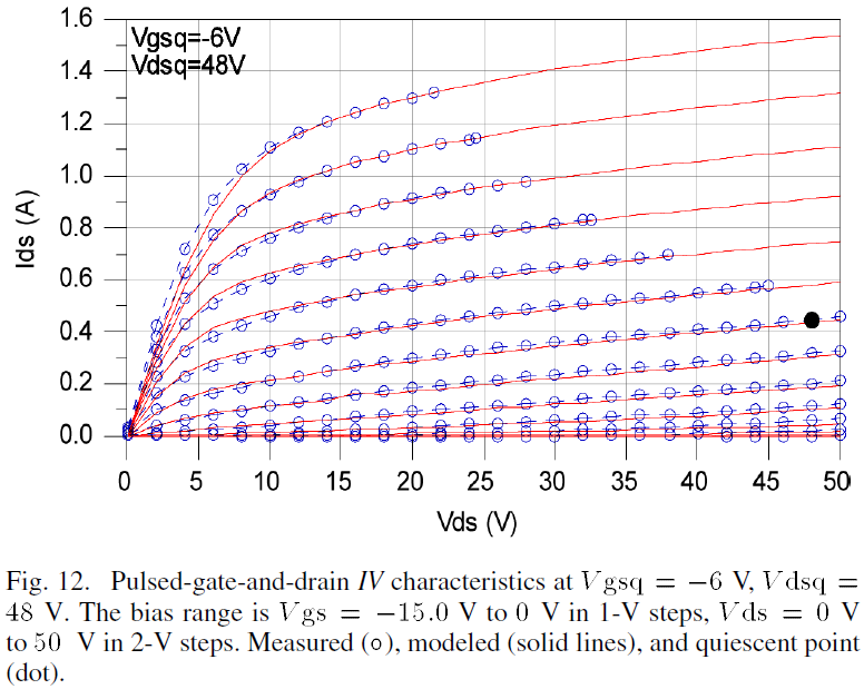
The performance of the model is also validated by comparing pulsed-gate-and-drain IV data with model predictions computed using transient simulations. The modeled and measured pulsed-gate-and-drain IV characteristics are shown in Figs. 10, 11 and 12 for quiescent biases at Vgsq=0V, Vdsq=0V, at Vgsq=-3V, Vdsq=30V and at Vgsq=-6V, Vdsq=48V, respectively. The results demonstrate that there is good agreement between the model output and measurements. Furthermore, this validates the trapping dispersion relationship developed in section II in which the effective gate-source voltage modification permits the drain current model derived from pulsed-gate IV characteristics to also predict pulsed-gate-and-drain IV characteristics.
In addition to the dynamic IV characteristics shown in Figs. 6-12, the model can also predict static IV curves. The measured versus modeled static IV characteristics from Vgs=-11.0V to -3.0V, Vds=0V to 58V are given in Fig. 13. Again, this demonstrates the validity of the temperature dependent drain current model presented in this work.
B. Small-Signal S-Parameters
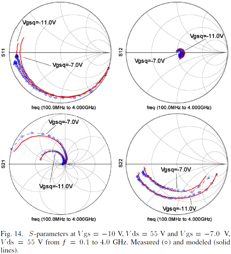
The S-parameters of the Cree SiC MESFET were measured over a range of bias points from Vgs=-10V to -5V in 1V steps for Vds=0V to 60V in 2V steps utilizing an HP 8510B vector network analyzer employing a microstrip TRL calibration from 0.1GHz to 4.0GHz. The S-parameters of the model compared with measured data for representative biases of Vgs=-10V, Vds=55V and Vgs=-7V, Vds=55V are shown in Fig. 14. An examination of these plots reveals a close agreement between the measured and modeled data, thus verifying the functionality of the model when employed in a small-signal mode.
To achieve good agreement betweenmodeled and measured S-parameters, many large-signal models use two drain current sources. One source models the DC drain current and the other operates at RF frequencies to compensate for differences between gm and gds derived at DC and those derived from S-parameters [7]. The RF current source provides supplementary current such that gm and gds are accurate under RF conditions, but this requires additional circuit characterization.
In this model, a single drain current source based on pulsed-gate IV characteristics and adapted for predicting pulsed-gate and pulsed-gate-and-drain IV characteristics is used. According to the comparison with S-parameter data, this current source, along with appropriately modeled parasitic elements can accurately predict the small-signal behavior of the device without using an RF current generator.
C. Output and Input Reflected Harmonic Power Versus Incident Power and Versus Bias
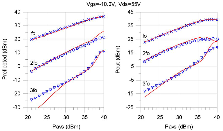
The fidelity of the power performance of the model is verified by comparing its output and input reflected predictions with measured power data. The transmitted output and input reflected power of the device at fo=2GHz over an available power range of 21dBm to 40dBm in 1dBm steps for two biases, Vgsq=-10.0V, Vds=55V and Vgsq=-7.0V, Vds=55V, are simulated and compared with measured data as shown in Figs. 15 and 16, respectively.
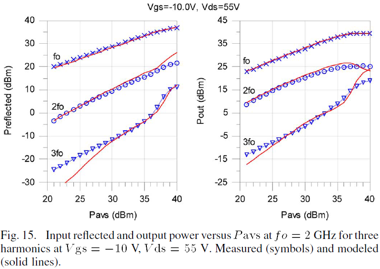
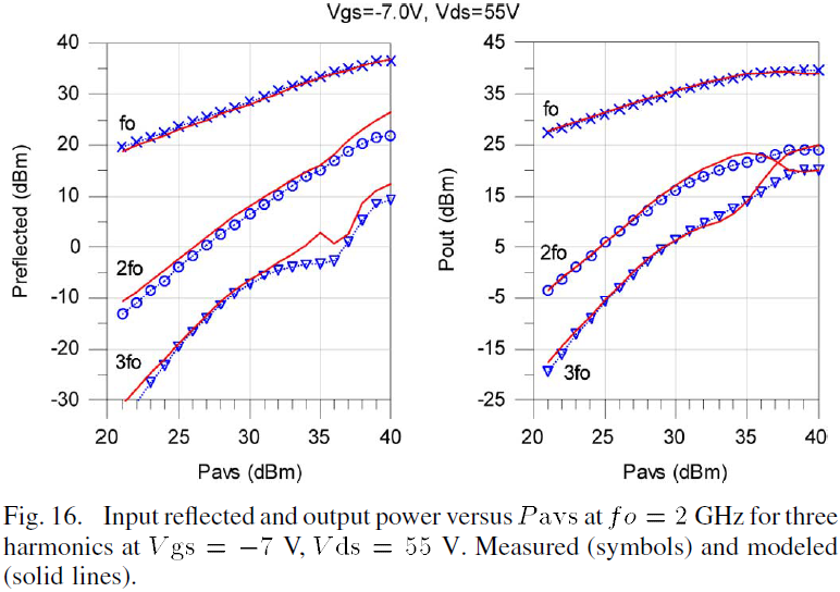
According to the output power characteristics shown in Figs. 15 and 16, the model provides a very good prediction of the output power for the first three harmonics for the two representative gate biases. In addition, the input power reflected from the gate for the first three harmonics also shows good agreement with the measured data as shown in Figs. 15 and 16. The input reflected power measurements can be used to compute the actual power delivered into the device which may be helpful in understanding and improving the efficiency of high power circuits.
Measuring and characterizing the harmonic power generation at both ports provides a better understanding of the device nonlinearities such as the terminal impedances and harmonic generation under large-signal excitation. The power measurements are of the unmatched device and not of a particular amplifier implementation, which further establishes this as a general device model.
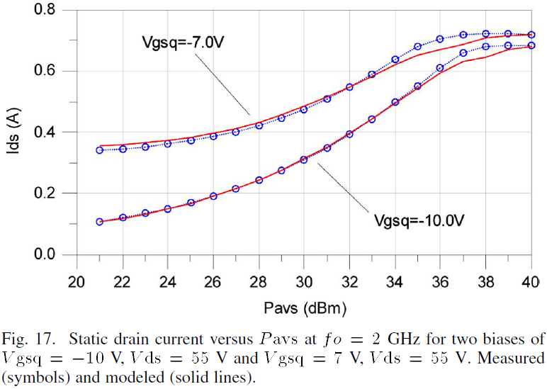
Under large-signal CW drive, the device will experience an increased static drain current due to large-signal nonlinearities and clipping. As a result the static drain current rises with increasing incident RF power. This effect leads to changes in the static dissipated power and thus creates variations in device temperature. A well developed thermal model is necessary to predict this change in static drain current. The modeled and measured static drain current versus incident power from 21dBm to 40dBm is shown in Fig. 17 for the biases of Vgs=-10V, Vds=55V and Vgs=-7V, Vds=55V. The model shows good agreement with the measured data signifying that it is capable of predicting the changes in static Ids with increasing RF drive power and the saturation of static Ids at high power levels.
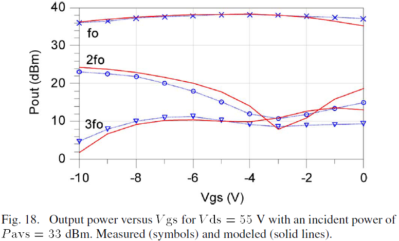
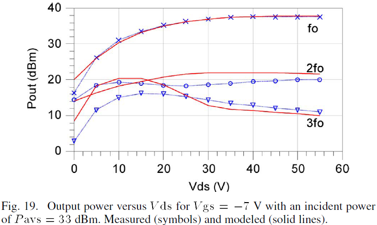
Additional characterization of the large-signal behavior of the device versus bias was performed in which the output power is measured across gate-source and drain-source voltages. The output power curves are shown as a function of Vgs and Vds in Figs. 18 and 19, respectively. The model shows good agreement with the measured data for three harmonics.
D. Large-Signal Power Versus Frequency
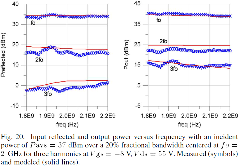
The large-signal performance of the model versus frequency has been assessed over a moderate band of frequencies. Fig. 20 shows modeled and measured data over a frequency range which covers the GSM 1800, GSM 1900, CDMA 1900, WCDMA 1900 and WCDMA 2100 commercial communications bands. This represents a range of 20% fractional bandwidth centered around 2 GHz with the device biased at Vgs=-8V and Vds=55V. A perusal of the data and model computations demonstrates the efficacy of the model in predicting output and input reflected power for three harmonics over this frequency range.
E. Third-Order Intermodulation Distortion
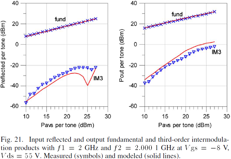
The third-order intermodulation distortion of the device has been characterized using a two-tone test which was conducted on the device with f1=2GHz and f2=2.0001GHz over an incident power range of 10dBm to 27dBm per tone with the device biased at Vgs=-8.0V, Vds=55V. Since the device is unmatched, significant third-order intermodulation products will be generated at both the output and input reflected ports. The measurement and modeled third-order intermodulation power is shown in Fig. 21. According to the data and simulated output, the model is capable of accurately predicting both output and input reflected third-order intermodulation products.
IV. Conclusions
A large-signal model for SiC MESFETs with a self-heating thermal model is presented here. A generalized current equation based on the Chalmers model, a thermal relationship and a trapping correctional model are presented. The drain current model has demonstrated the ability to model pulsed-gate IV characteristics and pulsed-gate-and-drain IV characteristics under various quiescent biases as well as static IV characteristics. The large-signal model has been implemented in Agilent ADS and can accurately predict the small-signal S-parameters and the large-signal output and input reflected power of the device for three harmonics across bias and frequency. The large-signal model has also demonstrated the model’s capability in predicting third-order intermodulation distortion.
Acknowledgment
The authors would like to thank Dr. Iltcho Angelov for his suggestions, Dr. Ahmed Sayed, Dr. David McQuate, Dr. Giovonnae Anderson and Dr. Wayne Martin for their generous contributions and support of this work.
References
[1] A. Sayed, “Ultra Wideband 5 W Hybrid Power Amplifier Design Using Silicon Carbide MESFETs,” M.S. Thesis, Technical University of Berlin, Berlin, Germany, 2005.
[2] R.A. Sadler, S.T. Allen, W. L. Pribble, T.S. Alcorn, J.J. Sumakeris and J.W. Palmour, “SiC MESFET hybrid amplifier with 30-W output power at 10 GHz,” IEEE/Cornell Conference on High Performance Devices, 2000. pp. 173 – 177, Aug. 2000.
[3] K. Andersson, V. Desmaris, J. Eriksson, N. Rorsman and H. Zirath, “C-band linear resistive wide bandgap FET mixers,” Microwave Symposium Digest, 2003 IEEE MTT-S International Volume 2. pp. 1303-1306, June 2003.
[4] Z.D. Schwartz, G.E. Ponchak, “1-GHz, 200/spl deg/C, SiC MESFET Clapp oscillator,” IEEE Microwave and Wireless Components Letters, Volume 15, Issue 11. pp. 730-732, Nov. 2005.
[5] I. Angelov, H. Zirath, N. Rorsman, , “A New Empirical Nonlinear Model for HEMT and MESFET Devices,” Microwave Theory and Techniques, IEEE Transactions on, vol. 40, no. 12, pp. 2258-2266. Dec. 1992.
[6] I. Angelov, L. Bengtsson, M. Garcia, “Extensions of the Chalmers nonlinear HEMT and MESFET model,” Microwave Theory and Techniques, IEEE Transactions on, vol. 44, pp. 1664 – 1674, Oct. 1996.
[7] I. Angelov, N. Rorsman, J. Stenarson, M. Garcia and H. Zirath, “An Empirical Table-Based FET Model”, IEEE Transactions on Microwave Theory and Techniques, Vol. 47, No. 12, pp. 2350 – 2357, Dec. 1999
[8] A. Sayed, G. Boeck, “An empirical large signal model for silicon carbide MESFETs,” Gallium Arsenide and Other Semiconductor Application Symposium, 2005. pp. 313-316, Oct. 2005.
[9] I. Angelov, V. Desmaris, K. Dynefors, P.A. Nilsson, N. Rorsman, H. Zirath, “On the large-signal modeling of AlGaN/GaN HEMTs and SiC MESFETs,” Gallium Arsenide and Other Semiconductor Application Symposium, 2005. EGAAS 2005. pp. 309-312. 3-4 Oct. 2005.
[10] I. Angelov, A. Inoue, T. Hirayama, D. Schreurs and J. Verspecht, “On the Modelling of High Frequency and High Power Limitations of FETs”, INMMiC Workshop, Rome, Italy, 4 p., 15-16 November 2004.
[11] I. Angelov, K. Andersson, D. Schreurs, D. Xiao, N. Rorsman, V. Desmaris, M. Sudow, H. Zirath, “Large-signal modelling and comparison of AlGaN/GaN HEMTs and SiC MESFETs”, Asia-Pacific Microwave Conference, 2006, pp. 279-282. 12-15 Dec. 2006.
[12] K. Yuk, G. R. Branner, “A Simplified, Empirical Large-Signal Model for SiC MESFETs,” European Microwave Integrated Circuits Conference, 2007. pp. 44-47, Oct 2007.
[13] F. Filicori, G. Vannini, A. Santarelli et al, “Empirical Modeling of Low-Frequency Dispersive Effects Due to Traps and Thermal Phenomena in III-V FET’s,” IEEE Transactions on Microwave Theory and Techniques, Vol. 43, No. 12, December 1995, pp. 2972-2981.
[14] T. Fernandez, Y. Newport, J. Zamanillo, A. Tazon, A. Mediavilla, “Extracting a Bias-Dependent Large Signal MESFET Model from Pulsed I/V Measurements,” IEEE Transactions on Microwave Theory and Techniques, Vol. 44, No. 3, March 1996, pp.372-378.
[15] T. Fernandez, J. A. Garcia, A. Tazon, A. Mediavilla, J. C. Pedro, J. L. Garcia, “Accurately Modeling the Drain to Source Current in Recessed Gate P-HEMT Devices,” IEEE Electron Device Letters, Vol. 20, No. 11, November 1999, pp.557-559.
[16] M. Chaibi, T. Fernandez, J. Rodriguez-Tellez, J.L. Cano and M. Aghoutane, “Accurate large-signal single current source thermal model for GaAs MESFET/HEMT,” Electronics Letters, Vol. 43, No. 14, July 5 2007.
[17] A. Hammache, G. Brassard, M. Bouchard, F. Beauregard, C. Akyel and F. M. Ghannouchi, “Thermal Characterization of MESFETs Using I-V Pulsed and DC Measurements,” IEEE Instrumentation and Measurement Technology Conference, May 1997, pp.664 – 667.
[18] M. Guyonnet, R. Sommet, R. Quere, G. Bouisse, “Non-Linear Electro Thermal Model of LDMOS Power Transistor Coupled to 3D Thermal Model in a Circuit Simulator,” 34th European Microwave Conference, Vol. 2, Oct 2004, pp. 573-576.
[19] Cree, Inc, “CRF24010 10W SiC RF Power MESFET datasheet,” available at http://www.cree.com/products/pdf/CRF24010-Rev1_4.pdf
[20] Cree, Inc, “Large Signal Models for Cree SiC MESFETs,” available at http://www.sekitech.co.jp/product/compo/pdf/CREE_Lightboxes_24x36.pdf
[21] R. Pengelly, “A Comparison between Class E Power Amplifiers employing LDMOS FETs and SiC MESFETs,” available at http://www.cree.com/products/pdf/A%20Comparison%20between%20Class%20E%20Power%20Amplifers%20employing%20LDMOS%20FETs%20and%20SiC%20MESFETs.pdf, Wireless and Microwave Technology Conference proceedings, 15 April 2004.
[22] P. Ladbrooke, Pulsed IV Measurement of Semiconductor Devices, Accent Optical Technologies, pp. 1-9 to 1-18.
[23] H. Fukui, “Thermal Resistance of GaAs Field-Effect Transistors,” International Electron Devices Meeting 1980, Vol 26., 1980, pp.118-121.
[24] D. Estreich, “A DC Technique for Determining GaAs MESFET Thermal Resistance,” IEEE Transactions on Components, Hybrids, and Manufacturing Technology, Vol. 12, No. 4, December 1989, pp. 675 – 679.
[25] N. Bovolon, P. Baureis, J.-E. Muller, P. Zwicknagl, R. Schultheis and E. Zanoni, “A Simple Method for The Thermal Resistance Measurement of AlGaAs/GaAs Heterojunction Bipolar Transistors,” IEEE Transactions on Electron Devices Vol. 45, No. 8, August 1998, pp.1846 – 1848.
[26] S. Marsh, “Direct Extraction Technique to Derive the Junction Temperature of HBT’s Under High Self-Heating Bias Conditions,” IEEE Transactions on Electron Devices, Vol. 47, No. 2, February 2000, pp. 288-291.
[27] J.C.J. Paasschens, S. Harmsma, and R. van der Toorn, “Dependence of Thermal Resistance on Ambient and Actual Temperature,” Bipolar/BiCMOS Circuits and Technology, 2004. Sept. 2004. pp. 96-99.
[28] I. Angelov, Camilla Karnfelt, “Direct Extraction Techniques for Thermal Resistance of MESFET and HEMT Devices,” IEEE Radio Frequency Integrated Circuits Symposium, 2007. June 2007. pp. 351 – 354.
[29] D. Siriex, D. Barataud, R. Sommet, O. Noblanc, Z. Ouarch, C. Brylinski, J.P. Teyssier, R. Quere, “Characterization and modeling of nonlinear trapping effects in power SiC MESFETs,” IEEE MTT-S Internaational Microwave Symposium Digest, Vol. 2, pp. 765-768, June 2000.
[30] Nanometrics, “DiVA [Dynamic I-V Analyzer],” available at http://www.nanometrics.co.kr/products/Diva.html
[31] Z. Ouarch, J.M. Collantes, J.P. Teyssier, R. Quere, “Measurement Based Nonlinear Electrothermal Modelling of GaAs FET with Dynamical Trapping Effects,” IEEE MTT-S International Microwave Symposium Digest, Vol. 2, pp. 599-602, June 1998.
[32] K. Kunihiro, Y. Ohno, “A large-signal equivalent circuit model for substrate-induced drain-lag phenomena in HJFETs,” IEEE Trans. on Electron Devices, Vol 43, no. 9, Sept. 1996, pp.1336-1342.
[33] R. Anholt, Electrical and Thermal Characterization of MESFETs, HEMTs, and HBTs. Boston, Artech House, 1995, pp.36-44.
[34] G. Dambrine, A. Cappy, F. Heliodore and E. Playez, “A new method for determining the FET small-signal equivalent circuit,” IEEE Transactions on Microwave Theory and Techniques, vol. 36, July 1988, p. 1151-1159.
[35] H. Fukui, “Determinations of the basic parameters of a GaAs MESFET,” Bell Systems Technical Journal, Vol. 58, no. 3, Mar. 1979.