

 0
0
 0
0
By Kelvin Yuk, G. R. Branner and David McQuate
First appears: IEEE MTT-S Int. Microw. Symp., pp. 753-756, Jun. 2009.
A new empirical large-signal model for high-power GaN HEMTs utilizing an improved drain current (Ids) model is presented. The new Ids formulation accurately predicts the asymmetric bell-shaped transconductance (gm) over a large drain-source bias range which is crucial in modeling high-power GaN HEMTs. A method of utilizing a combination of pulse-gate (PGIV) and pulsed-gate-and-drain (PIV) IV measurements to characterize the dispersive behavior of GaN HEMT nonlinear Ids characteristics is developed. Dispersion due to self heating is modeled by modifying Ids parameters as a function of the temperature change and drain-source bias. Dispersion due to trapping is modeled using an effective gate-source voltage model. Accurate predictions of the RF small-signal and large-signal performance are demonstrated for two quiescent biases.
I. Introduction
AlGaN/GaN high electron mobility transistors (GaN HEMT) are emerging as a frequently employed technology in high power RF circuits. This is primarily due to desirable attributes such as high drain-source current, high drain-source breakdown voltage and wideband RF operation. As a result, these devices show great promise in the development of compact, high power microwave circuits. An accurate nonlinear model is essential in designing applications for GaN HEMTs such as high efficiency and broadband power amplifiers. However, some of the challenges in modeling GaN HEMTs arise from the presence of current dispersion due to thermal self-heating and charge trapping. Thermal heating is a product of the device’s high power density while charge trapping is due to the relatively new GaN processing technology. These dispersive phenomena can drastically alter the RF performance of the device and this further complicates the characterization and modeling process.
Recent work in GaN HEMT empirical modeling includes [1]-[3] which address IV modeling and the dispersive effects on RF device performance. In the current work, several of the techniques suggested in [4] and employed in the development of a SiC model in [5] will be used to develop an improved high-power GaN HEMT model. This provides a model which accurately characterizes the dispersive nonlinear drain current (Ids), small-signal and large-signal RF behavior of high-power GaN HEMTs. A new Ids model accounting for self-heating and charge-trapping will be presented for high power GaN HEMTs. The model thus allows predictions of pulsed-gate IV (PGIV) and pulsed-gate-and-drain IV (PIV) characteristics under various quiescent gate-source (Vgsq) and quiescent drain-source (Vdsq) biases.
The device studied in this work is the Cree Inc. CGH40010F 10W RF Power GaN HEMT [6]. In obtaining the measured data presented, the device was mounted on an aluminum plate secured to a heat sink and fan which permits efficient transfer of heat generated from the device under high power dissipation. The empirical circuit model is implemented and simulated using the Agilent Advanced Design System (ADS) software.
In Section II, the complete model will be described including the new Ids representation incorporating the effects of self-heating and trapping along with PGIV and PIV data. In Section III, the RF performance of the model will be presented and compared with extensive measured S-parameters, large-signal input-reflected and output harmonic power. Section IV will conclude this work.
II. Model Description
The complete nonlinear model with thermal subcircuit is shown in Fig. 1. This representation incorporates the nonlinear Ids source, bias-dependent gate-source (Cgs), gate-drain (Cgd) and drain-source (Cds) capacitances, gate-source (Dgs) and gate-drain (Dgd) nonlinear diodes and linear parasitic package resistances, inductances and capacitances.
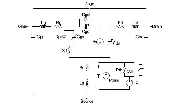
Fig. 1. Complete large-signal model schematic.
In the following presentation, the development of the Ids model will be described first (Section II.A). This will be followed by the thermal (Section II.B) and trapping models (Section II.C), extrinsic and intrinsic parasitics (Section II.D) and nonlinear diodes (Section II.E).
A. Drain Current Characterization and Modeling
The Chalmer’s model has been shown to provide excellent predictions of HEMT drain current behavior by accurately modeling the transconductance of the device [7]. A modified version of the model presented in [4], is used for modeling the Ids of the high-power GaN HEMT. This is given by (1) as:

where Pn are the coefficients of the Ψ polynomial and MIpk is a multiplier for Ipk defined by the expression presented in (2):

One crucial aspect of developing an Ids model is to accurately represent the highly asymmetric bell-shaped transconductance (gm) of the device. Measured and modeled values of gm are represented in Fig. 2. This process is performed in two steps. First, each polynomial term of Ψ in (1) has a unique Vpk value [4]. Secondly, MIpk, a multiplier term for Ipk, is introduced in (2). In previous implementations of the Chalmers model, MIpk=1 and the maximum drain current is equal to 2Ipk. The introduction of MIpk permits the drain current to increase beyond 2Ipk as a function of Vgs as shown in Fig. 2. In turn, MIpk elongates the asymmetry of gm for Vgs>Vpk. The drain-source voltage relationships for parameters Pn and MIpkb shown in (1) and (2), respectively, permit Ids and the gm bell shape to transition between the linear and saturation regions.
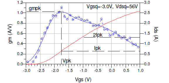
Fig. 2. Transconductance (blue) and Ids (red) vs Vgs at Vgsq= 3.0V, Vdsq=56V illustrating highly asymmetric characteristic.
The development of the eventual large-signal model first proceeds by employing PGIV data. The Ids representation of (1) and (2) is first employed to model the PGIV device characteristics with a quiescent gate bias below pinchoff at Vgsqpinch=-3.0V as shown in Fig. 3. Very high power PGIV characteristics are straightforward to obtain and can completely describe the thermal behavior of a device using a limited subset of Vgsq biases [5]. The PGIV set at Vgsqpinch=‑3.0V has zero power dissipation and will serve as a basis for the final Ids modeling. The resulting Ids model based on this PGIV data can then be appropriately modified to incorporate thermal heating and trapping effects.
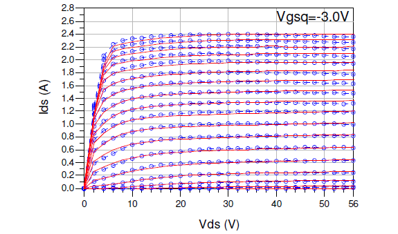
Fig. 3. Measured (circles) and modeled (solid lines) PGIV characteristics at Vgsq=-3.0V for Vgs=-2.7V to 0.7V, 0.2V steps and Vds=0V to 56V, 2V steps.
B. Modeling of Dispersive Phenomena Due to Self-heating
The thermal circuit shown in Fig. 1 provides a means to model the thermal behavior of the device. The device temperature T is described by the formula:

where T0 is the ambient temperature, ΔT’ is the time-varying temperature change and is the thermal time constant.
The temperature-sensitive parameters of (1) and (2) were determined by fitting several sets of PGIV characteristics at different Vgsq where the device experiences self-heating. The thermal relationship of these parameters, Ipk, P1, P2, P3 in (1) and MIpkb in (2) can each be modeled as a function of the temperature change and drain-source voltage by

where Param is the respective parameter under zero power dissipation, and and are drain-source voltage fitting parameters. The efficacy of the outcome of this process is shown in Fig. 4. A modeled set of PGIV characteristics at Vgsq=-1.7V shown in Fig. 4 demonstrates the ability of the Ids equation to accurately predict the effects of self-heating using the above temperature-modified parameter relationships.
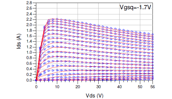
Fig. 4. Measured (circles) and modeled (solid lines) PGIV characteristics at Vgsq=-1.7V for Vgs=-2.7V to 0.7V, 0.2V steps and Vds=0V to 56V, 2V steps.
C. Modeling of Dispersive Phenomena Due to Trapping
Substrate trapping effects in the GaN HEMT are observable by comparing the PIV characteristics at different quiescent points. This is illustrated by a comparison of Ids values at Vgsq=0V, Vdsq=0V (Fig. 5a), Vgsq=-3V, Vdsq=0V (Fig. 5b) with those at Vgsq=-3V, Vdsq=28V (Fig. 5c). Surface traps reduce the effectiveness of the applied Vgs while substrate traps give rise to a backgate voltage which further decreases the effective value of Vgs [5]. The Ids expression in (1) was applied to PGIV characteristics and therefore includes the effects of static surface trapping determined by Vgsq and those of static substrate trapping determined by Vdsq. These effects can be extracted from the Ids computation by modifying Vgs for surface traps and for substrate traps as done previously in a successful SiC model development [5]. For the current GaN model, the expressions are given in (4) as:

where γsurf and γsubs are the surface and substrate trapping parameters, respectively.
Figs. 5a-5d show PIV characteristics for four different quiescent bias conditions. Comparison of the PIV characteristics presented at Vgsq=0V, Vdsq=0V (Fig. 5a) and at Vgsq=-3V, Vdsq=0V (Fig. 5b) illustrate the efficacy of the surface trapping modification in (4). Comparison of the PIV characteristics presented at Vgsq=-3V, Vdsq=0V (Fig. 5b) and at Vgsq=-3V, Vdsq=28V (Fig. 5c) illustrate the efficacy of the substrate trapping modification in (4). The PIV characteristics at Vgsq=-1.7V, Vdsq=28V (Fig. 5d) demonstrate that both trapping and self-heating models working simultaneously can provide an excellent match.
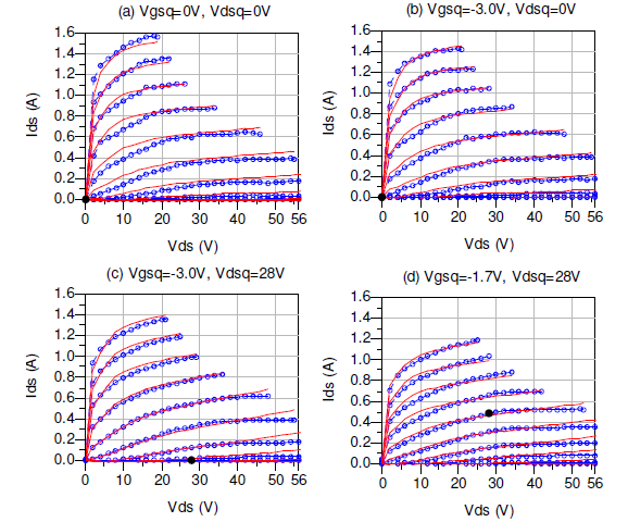
Fig. 5. Measured (circles) and modeled (solid lines) PIV characteristics at biases (dots) (a)Vgsq=0V, Vdsq=0V (b)Vgsq=-3V, Vdsq=0V, (c)Vgsq=-3V, Vdsq=28V, (d)Vgsq=-1.7V, Vdsq=28V for Vgs=-3V to -0.75V, 0.25V steps, Vds=0V to 56V, 2V steps.
D. Small-signal Extrinsic and Intrinsic Parasitic Extraction and Modeling
The extrinsic and intrinsic resistances, inductances and capacitances of the model (Fig. 1) were extracted from multibias S-parameter measurements using standard methods. The extracted multibias Cgs, Cgd and Cds were implemented using the charge-equation based nonlinear capacitance model [7].
E. Nonlinear Gate-source and Gate-drain Diodes
The nonlinear gate-source and gate-drain diodes were measured using forward bias IV measurements and modeled using the Shockley ideal diode equation.
III. Experimental Model Verification Under RF Drive
The RF performance of the model compared with measured data is presented in Section III.A. and Section III.B. below. Both small-signal and large-signal RF comparisons will be illustrated at two quiescent biases, Vgsq=-2.5V, Vdsq=28V and Vgsq=-1.9V, Vdsq=28V, to demonstrate the efficacy of the dispersion modeling process developed in this work.
A. Small-signal S-parameters
The measured and modeled S-parameters of the GaN HEMT for the two biases over a frequency range of 0.2GHz to 10GHz are shown below in Fig. 6 and Fig. 7. The accurate prediction of the S-parameters using the GaN HEMT model presented shows the validity of the Ids implementation under small-signal operation. A perusal of the S-parameter values reveals that the model can provide very good predictions for frequencies up to 10GHz.
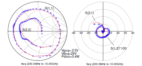
Fig. 6. Measured (circles) and modeled (solid lines) S-parameters for 0.2GHz to 10.0GHz at Vgsq=-2.5V, Vdsq=28V
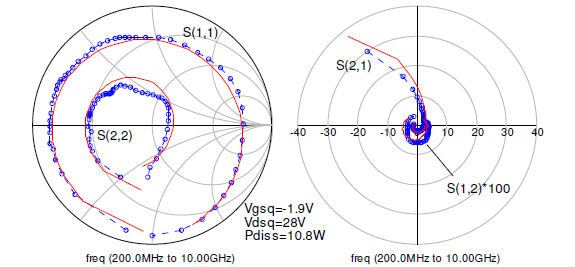
Fig. 7. Measured (circles) and modeled (solid lines) S-parameters for 0.2GHz to 10.0GHz at Vgsq=-1.9V, Vdsq=28V.
B. Large-signal Harmonic Power at Gate (Input Reflected) and Drain (Output) Ports
The input reflected (Prefl) and output generated (Pout) harmonic power were measured over an available source power (Pavs) ranging from +20dBm to +39dBm at a frequency fo=3.333GHz under 50 ohm terminations. A comparison of these measured and modeled results in Fig. 8 and Fig. 9 demonstrates that the model has shown the ability to closely predict the nonlinear behavior at the two biases. The complete nonlinear model presented here and its accurate predictions support its value in studying the behavior and control of harmonics in microwave GaN HEMT circuits.
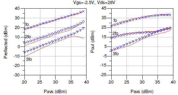
Fig. 8. Measured (symbols) and modeled (solid lines) Prefl vs. Pavs and Pout vs. Pavs for fo=3.333GHz at Vgsq=-2.5V, Vdsq=28V.
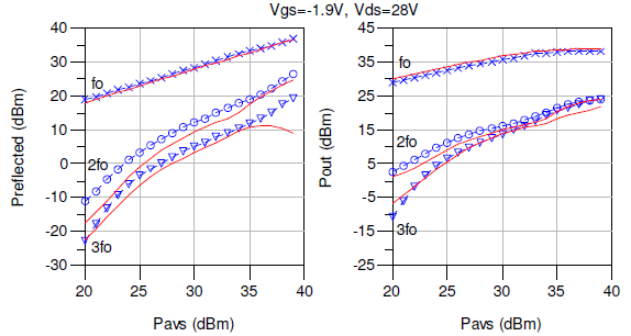
Fig. 9. Measured (symbols) and modeled (solid lines) Prefl vs. Pavs and Pout vs Pavs for fo=3.333GHz at Vgsq=-1.9V, Vdsq=28V.
IV. Conclusion
A large-signal drain current model capable of modeling the dynamic IV characteristics of high-power GaN HEMTs is presented. The complete model with parasitics and nonlinear capacitances has shown the ability to accurately predict the behavior of the device under small-signal over a very large bandwidth and large-signal operation for three harmonics.
Acknowledgement
The authors wish to acknowledge Dr. I. Angelov for his advice, Dr. W. Martin and Dr. G. Anderson.
References
[1] I. Angelov, V. Desmaris, K. Dynefors, P. A. Nilsson, N. Rorsman, and H. Zirath, “On the large-signal modeling of AlGaN/GaN HEMTs and SiC MESFETs,” Gallium Arsenide and Other Semicond. Appl. Symp., pp. 309–312, Oct. 2005.
[2] G. Torregrosa, J. Grajal, M. Peroni, A. Serino, A. Nanni and A. Cetronio, “Large-Signal Modeling of Power GaN HEMTs Including Thermal Effects,” in European. Microwave Integrated Circuits Conf., pp. 36–39, Oct. 2007.
[3] O. Jardel, F. De Groote, T. Reveyrand, et al, “An Electrothermal Model for AlGaN/GaN Power HEMTs Including Trapping Effects to Improve Large-Signal Simulation Results on High VSWR,” IEEE Trans. Microwave Theory & Tech., vol. 55, no. 12, pp. 2660-2669, Dec. 2007.
[4] I. Angelov, D. Schreurs, “Empirical Device Models,” in IMS2007 Workshop, Advances in Active Device Char. & Modeling for RF and Microwave, June 4, 2007.
[5] K. S. Yuk and G. R. Branner, “An Empirical Large-Signal Model for SiC MESFETs With Self-Heating Thermal Model,” IEEE Trans. Microwave Theory & Tech., vol. 56, no. 11, pp. 2671-2680, Nov. 2008.
[6] “CGH40010 10W, RF Power GaN HEMT datasheet,” Cree, Inc., Durham, NC, 2007. [Online]. Available: http://www.cree.com/products/pdf/CGH40010.pdf
[7] I. Angelov, N. Rorsman, J. Stenarson, M. Garcia and H. Zirath, “An Empirical Table-Based FET Model”, IEEE Trans. Microwave Theory & Tech., Vol. 47, No. 12, pp. 2350 – 2357, Dec. 1999.