


 0
0
 0
0
Published at WAMICON on April 25, 2017
J. Tan, K. S. Yuk, and G.R. Branner
Dept. of Electrical and Computer Engineering
University of California at Davis
Davis, USA
Abstract
A wideband Gallium Nitride (GaN) HEMT power amplifier (PA) achieving 7.6W output power over 1.1 GHz bandwidth at fo=2.75 GHz is presented. A systematic design and synthesis of wideband low-pass matching networks realizing optimal fundamental impedance is applied. These techniques have produced amplifiers with increased output power, efficiency and very large fractional bandwidth. Additionally, the PA can achieve a maximum 61% power added efficiency. This work seeks to maximize the usable bandwidth of the GaN HEMT PA to the maximum possible operating frequency.
I. Introduction
Power amplifiers are a vital component in virtually all RF systems and specifically in modern RF transceiver systems [1]. Due to demanding specifications for output power, linearity, efficiency and bandwidth, strides to improve power amplifier performance as a discrete subsystem will continue for the foreseeable future. However, often the design tradeoffs between these performance parameters in addition to size, weight, and technology limitations create many challenges for PA design. Broadband amplifiers specifically have many applications such as in instrumentation, electronic warfare, high-resolution radar, and broadband radio transceivers.
In this work, a broadband technique based on filter design is used to determine the maximum achievable bandwidth of a GaN HEMT, while still retaining 7.6W output power and a reasonably high PAE. The input and output matching networks are designed using Chebyshev lowpass impedance-transforming filters with an octave bandwidth at S-Band. These filters are then modified to provide the proper reactive impedance match across the desired band, as described in [2] for the case of a Class E switching amplifier. Adapting these techniques for a general continuous-mode PA seeks to explore their applications at a higher frequency range and without encountering the disadvantages inherent to switched-mode amplifiers, such as the high voltage swing across the device and the corresponding required increase in DC power supply capacity [1].
The networks are realized using distributed microstrip elements. The finished PA produces 38.8 dBm output power with a minimum power added efficiency (PAE) of 40% over a bandwidth of 1.1 GHz centered at 2.75 GHz. The 1100 MHz bandwidth achieved by this PA is both larger and at a higher center frequency than other recently published work.
The characterization of the GaN HEMT in simulation and the PA design strategy involving the bias selection and load and source networks design is described in Section II. Small-signal and large-signal measured performance of the synthesized networks and overall power amplifier is provided in Section III. Finally, Section IV presents the primary conclusions of this development.
II. Design of High Efficiency Power Amplifiers
The primary performance parameters under investigation for this PA research are:
1. Output power
2. Bandwidth
3. Power added efficiency (PAE)
As stated in Section I, a primary objective for this design is to investigate the maximum achievable bandwidth for a high-efficiency PA while retaining good power performance at S-band frequencies (2-4GHz). Covering a wide variety of commercial applications including telecommunications, radar, and general-purpose instrumentation, this frequency coverage has many benefits.
In this work, the commercially available and widely studied CGH40010F 10W GaN HEMT device manufactured by Wolfspeed, a subsidiary of Cree Inc., is used for the PA design. A non-linear device model provided by the manufacturer was used for simulations using the Keysight Advanced Design System (ADS) microwave design software. This model has shown to be accurate for high-efficiency PA designs, although other advanced GaN HEMT models have been developed [3]. The microwave substrate used for the design is 20mil Rogers RT/duroid 5880 microwave laminate, chosen for its high performance characteristics at the targeted frequencies.
The detailed design of the GaN HEMT-based microwave power amplifiers is described from the primary design steps: (a) the selection of the appropriate device biasing, (b) the determination of the source and load impedances for maximum bandwidth, Pout and PAE and (c) the synthesis of these impedances into compact, low-loss microstrip networks.
A. Device Biasing
Biasing of the gate and drain terminals is important step in ensuring high-efficiency operation of the PA. Initially, the device is biased in Class B, which corresponds to pinchoff or slightly below at the gate-source terminal. This will ensure zero quiescent current and complete self-biasing under RF drive. However investigation was made into biasing below Class B, in the Class C region, which can increase efficiency at the expense of output power and linearity.
Using extensive simulations, a gate voltage of Vgs= 3.6V is chosen as it provides a good tradeoff between power and efficiency. The maximum possible PAE and output power over the swept quiescent Vgs is shown in Fig. 1. A drain bias of Vds=28V is selected as it is the recommended voltage of the device. At this Vds, the device will have ample drain-source voltage swing under RF drive.
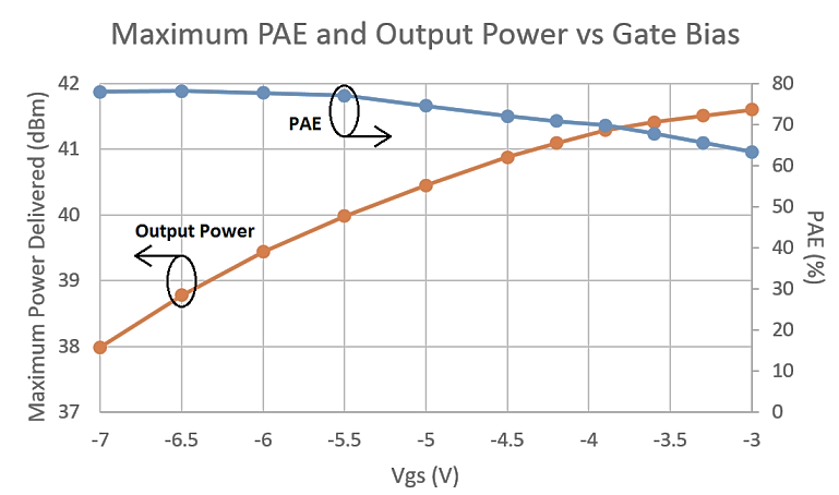
Fig. 1. Simulated maximum output power and maximum PAE vs quiescent gate bias.
B. Determination of Harmonic Load and Source Impedances
The first step in designing the source and load networks is to determine the impedance values at the source and load which are best suited for meeting the bandwidth, Pout and PAE requirements. An investigation of this is done by performing extensive load-pull simulations on the GaN HEMT large-signal model in ADS at specific fundamental frequencies across the entire 2-4GHz targeted operating band.
The analysis is performed once with an emphasis on Pout and again with an emphasis on PAE. The impedances at the gate with the device under the optimal load impedances are recorded and will serve as the design requirement for the source matching network. Since the input matching is to provide gain, a simple conjugate match of these impedances over the operating bandwidth are a satisfactory design criteria.
The resulting source and load impedances identified through the load-pull simulations are shown in Fig. 2 plots (a) and (b), respectively. The impedance values and resultant Pout and PAE are provided in Table I, which show a theoretically achievable efficiency of at least 67% and output power of at least 37 dBm across the entire S-band.
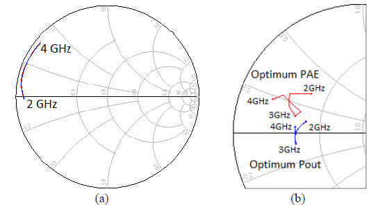
Fig. 2. Simulated (a) source impedances and (b) load impedances for the GaN HEMT over the desired bandwidth for maximum PAE (red) and maximum Pout (blue).
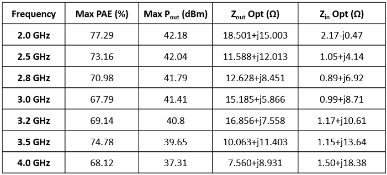
Table I. Optimal Load and Source Impedances
C. Synthesis of the Load and Source Network
Next, transforming filters are designed to realize the source and load impedances found in Section II.B. The load network has a greater effect on Pout and PAE and is therefore treated first followed by the design of the source network to increase gain. The matching networks are designed to transform from a 50-ohm termination.
A classical approach utilizing lumped-element lowpass Chebyshev ladder network is adopted for the network topology [4]. A lowpass structure is chosen instead of a bandpass structure because low-frequency out-of-band rejection is not required and can be traded-off for improved in-band ripple [3].
The order of the network is determined by three parameters: the real-to-real transformation ratio of the load to termination impedance, the fractional bandwidth (FBW), and the maximum in-band ripple. In the case of the load network, the real impedance at fo=3GHz is Re{Zout,opt}=15.185 ohms, giving a matching ratio of 3:1. For a FBW=0.8 and an in-band ripple of <0.1 dB, a 6-element network is chosen as shown in Fig. 3.
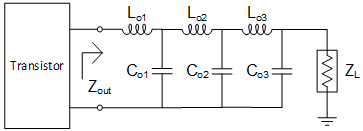
Fig. 3. Lumped-element lowpass output matching network.
Since the resulting filter performs a real-to-real-transformation only, it must be modified to provide the reactive component of Zout,opt. This is achieved by increasing the value of inductor L1 until the imaginary part of Zout,opt is obtained. The components are then tuned using ADS optimization until an optimal match across the band was established.
The next step is to convert the lumped-element design into a distributed transmission line realization. For the output network, a stepped-impedance topology with TL line impedances of 100 ohms (high-Z) and 20 ohms (low-Z) is used, which provided for easily realizable dimensions using the 20mil Rogers substrate. Since the high-Z line closest to the transistor was found to be too short in practice, its length is extended and its impedance reduced to maintain proper inductance value. It is also tapered out to 50 ohms in order to better contact the flange of the packaged transistor. Next, a DC bias network is incorporated into the design using a high-inductance 100-ohm feed line connected through bypass capacitors. The network is then re-tuned and optimized such that the desired impedance match is not altered. The circuit diagram and TL parameters of the distributed load network are shown in Fig. 4.
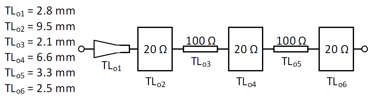
Fig. 4. Layout of the distributed stepped-impedance lowpass output matching network.
For the input network, a similar design approach is employed, however a much higher matching ratio is required due to the low value of Re{Zin,opt}=1 ohm. Because of the difficulty in achieving a 1-ohm match, an alternate target impedance of approximately 6 ohms was chosen which requires only an 8:1 ratio instead of a 50:1 ratio. Simulations predict only a minimal effect on the in-band amplifier performance from using the alternate 6-ohm input impedance. For the same FBW=0.8 and < 0.1 dB in-band ripple, an 8-element network was chosen. We found that although 8 elements are required by direct synthesis, the initial inductor and final capacitor values are eliminated when adjusting for the reactance of Zin,opt. As a result, the network reduces to a 6-element design as shown in Fig. 5.
Fig. 5. Lumped-element lowpass input matching network.
The input network is realized using transmission line stubs of 36 ohms to approximate the capacitors and high impedance 100-ohm lines to approximate the inductors, which again were chosen for ease of construction. One line, TLi3, is meandered due to its greater length. In the same manner as for the output network, a DC bias network is incorporated into the design and the network is re-optimized to achieve the best possible match. The circuit diagram of the source network is shown in Fig. 6.
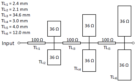
Fig. 6. Layout of the distributed lowpass input matching network.
The complete amplifier design was then optimized under harmonic balance with the active transistor model to maximize the Pout and PAE performance of the PA over the specified bandwidth. Lastly, ADS Momentum simulations are performed to verify and finalize the design prior to fabrication.
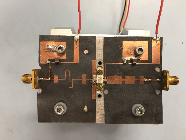
Fig. 7. The fabricated PA.
III. Measurements and Circuit Performance
The small-signal response of the input and output matching networks are measured on a network analyzer to validate the design. The in-band impedances of the input network, Zin,net, and the in-band impedances of the output network, Zout,net, are both shown in Fig. 8. It can be observed that the matching networks have properly realized the target impedances by the localization of S(1,1) on the Smith Chart when compared to the curves provided in Fig. 2.
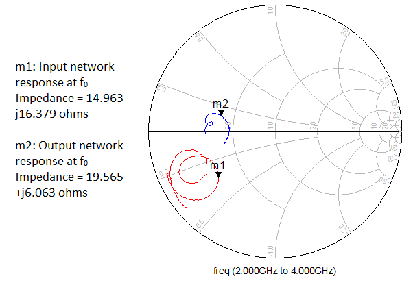
Fig. 8. S(1,1) measurements of the input matching network (red) and output matching network (blue).
The performance of the GaN HEMT-based amplifier was then measured under a variety of large-signal drive conditions. The Pout, PAE and gain vs input power at fo=2.7GHz is shown in Fig. 9. From the measured data, the PA clearly can achieve 40dBm (10W) output at Pin=22dBm for a gain of 17.8dB and PAE of 61.9%.
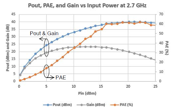
Fig. 9. Measured output power, gain, and PAE vs Pin at 2.7 GHz.
The Pout, PAE and Gain vs freq at Pin=25dBm measured from 2 to 3.5GHz is shown in Fig. 10. We can see that the PA output exhibits at least 38.8dBm power between 2.2 to 3.3GHz. Over that range, the PA is able to sustain PAE > 40%.
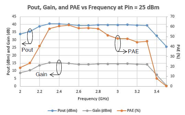
Fig. 10. Measured output power, gain, and PAE vs frequency.
The shape of the Pout vs Pin curve in Fig. 9 indicates the nonlinear behavior of the PA at backed-off power levels. This is possibly due to the Class C bias conditions and can be further explored and addressed through linearization techniques.
Table II compares the amplifier’s maximum performance at f0 with that of recently published work. The presented PA has a very high bandwidth and a maximum operating frequency that is higher than many by others using GaN devices.
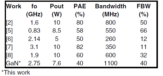
Table II. Performance Summary and Comparison
IV. Conclusion
The design of GaN HEMT-based high power, high efficiency wideband PAs has been investigated. A design approach utilizing extensive load-pull simulations and a network synthesis technique following the classical approach of [4] has been applied. The realized PA exhibits excellent performance under RF and is able to produce up to 10W with nearly 15 dB of gain while retaining > 40% PAE over 40% FBW, with a maximum PAE of 61%.
References
[1] S. C. Cripps, RF Power Amplifier for Wireless Communication, Second Edition, Artech House Publishers, 2006. [2] K. Chen, D. Peroulis, “Design of highly efficient broadband class-E power amplifier using synthesized low-pass matching networks,” IEEE Trans. MTT, vol. 59, no. 12, December 2011. [3] K. S. Yuk, G. R. Branner, and D. J. McQuate, “A wideband, multiharmonic empirical large-signal model for high-power GaN HEMTs with self-heating and charge-trapping effects,” IEEE Trans. MTT, vol. 57, no. 12, pp. 3322-3332, Dec. 2009. [4] G. Matthaei, “Tables of Chebyshev impedance-transforming networks of low-pass filter form,” Proceedings of the IEEE, pp. 939-963, August 1964. [5] V. Carrubba, J. Lees, J. Benedikt, P. J. Tasker, and S. C. Cripps, “A novel highly efficient broadband continuous class-F RFPA delivering 74% average efficiency for an octave bandwidth,” IEEE MTT-S IMS Digest, pp. 1-4, Jun. 2011. [6] Z. Wang, C. W. Park, “Novel wideband GaN HEMT power amplifier using microstrip radial stub to suppress harmonics,” IEEE MTT-S IMS Digest, pp. 1-3, Jun. 2012. [7] K. Chen, D. Peroulis, “A 3.1-GHz class-F power amplifier with 82% power-added-efficiency,” IEEE Microwave And Wireless Components Letters, vol. 23, no. 8, pp. 436-438, August 2013. [8] F. Yang, J. Lees, H. Choi, H. Yu, and P.J. Tasker, “Continuous class BJ Power Amplifier with DGS output matching,” IEEE MTT-S IMS Digest, pp. 1-4, Jun. 2014.