

 0
0
 0
0
By Kelvin Yuk, G.R. Branner
Originally appears: European Microwave Integrated Circuit Conference 2007, pp. 44-47, Oct. 2007.
A new, simplified empirical large-signal model for high power microwave SiC MESFETs is presented. A generalized drain current source equation is developed, allowing close predictions of both pulsed and static IV characteristics, which vary significantly due to current dispersion. The drain current source is based on pulsed IV measurements and accurately predicts the gm and gds without supplemental RF current source generators as typically used in other models. The model is shown to accurately predict the output and input reflected power over an available power range of +10dBm to +36dBm for three harmonics while maintaining the ability to compute the small-signal S-parameters.
I. Introduction
Research in silicon carbide microwave devices and circuits has been growing rapidly. Devices such as SiC MESFETs are becoming a viable solution to the growing demands of robust, high power microwave applications and have become increasingly competitive with other high power technologies like GaN. Some of the advantages of SiC MESFETs are its high power density and high drain-source breakdown voltage making it ideal for high power applications.
The typical target application for SiC MESFETs is in high power narrowband and broadband amplifiers as the output stage of a transmitter. A number of SiC MESFET amplifiers have been demonstrated [1] and SiC MESFET amplifiers generating greater than 30W at high frequencies have been reported [2]. Other possible circuit applications for SiC MESFETs such as mixers and oscillators have also been studied and developed [3],[4]. The advantage of using SiC MESFETs for these circuit applications is to combine high gain and power output with signal processing functionality, thereby eliminating the need for an amplification stage. For any high power circuit design, an accurate large-signal model is necessary to have but challenging to develop.
Some recent empirical large-signal SiC MESFET models based on the Chalmers model [5],[6] have been reported [7],[8]. The model in [7] has shown to accurately predict small-signal performance and power output for low power SiC MESFET devices. However, as a general purpose model for both GaN and SiC devices, it possesses an increased number of parameters and its predictions of dispersive phenomenon of SiC devices can be improved. The table-based model in [8] has shown excellent drain current and capacitance modeling results. However, it predicts large-signal power output of a specific amplifier implementation, lacking generality.
This paper presents a simplified empirically-based large-signal model capable of predicting the dc, small-signal and large-signal characteristics of the Cree CRF-24010 10W Silicon Carbide MESFET [9]. Unlike previous work, the output and input reflected power data of the unmatched device for three harmonics is provided and modeled accurately.
In Section II, the overall large-signal model is presented. A general, mathematically robust drain current model is described and implemented into a standard large-signal model topology. The complete model including small-signal parasitics, nonlinear capacitances and junction diodes is implemented in Agilent ADS. In Section III, the S-parameter and power performance of the model is verified with measured data. The model accurately predicts the small-signal S-parameters using only pulsed IV characteristics for the drain current source without using supplemental RF drain current sources as found in previous work. The model presented herein is shown to predict the output power and input reflected power over an available power range of 10dBm to 36dBm for three harmonics in good agreement with measured data. Conclusions are given in Section IV.
II. Model Description
The large-signal model is shown in Fig. 1.
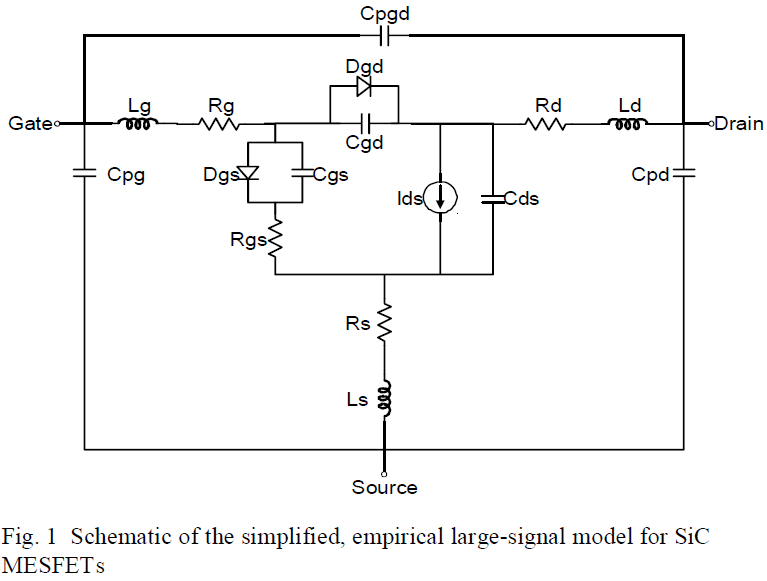
In all device measurements, the SiC MESFET was mounted on an aluminum plate fastened to a heat sink and fan for temperature reduction. The nonlinear elements of the model consist of the single drain-current source, Ids, the gate-source diode, Dgs, the gate-drain diode, Dgd, the gate-source capacitance, Cgs, the gate-drain capacitance, Cgd, and the drain-source capacitance Cds.
A. Large-Signal Drain Current Model
The standard Chalmers model assumes that the Ids dependence on Vgs and Vds are separable, that the nonlinear relationship between Ids and Vgs extends across the Vds range in a linear fashion and that the linear regime of the drain current can be modeled by multiplying the saturation current by a tanh(αVds) function [5]. While these approximations are applicable to low power devices, they may not be for high power devices that exhibit significant current dispersion. In devices such as SiC MESFET, the Ids dependence on Vds is not only nonlinear, but that relationship also changes with the applied Vgs. As a result, multiplication of Vgs-only dependent terms and the Vds-only dependent terms may not adequately describe the drain current due to this parameter interdependence. Another limitation is that the linear regime response may require a more sophisticated model for accuracy.
The drain current model used here is given in (1) and is an extension of the basic Chalmers model [5].
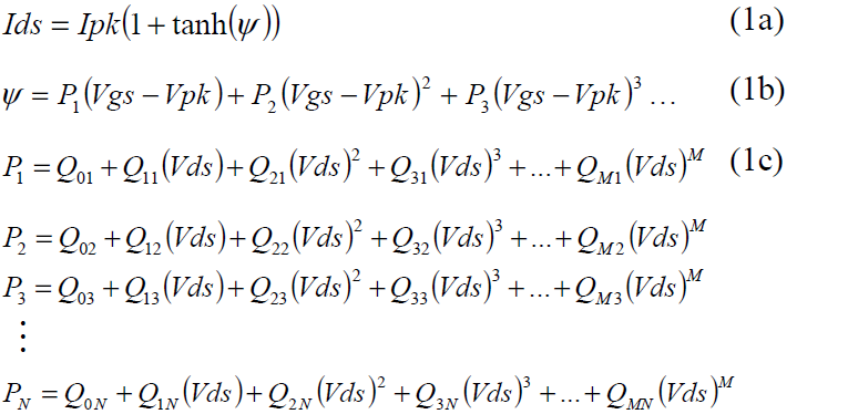
Here, the parameters of the power series describing the Vgs dependence are each a power series expansion of Vds. The key observation is the variation of gmpk as a function of Vds. By extracting Ipk and Vpk values across the Vds range, the polynomial coefficients Qmn can be solved in a way that describes the drain current behavior for all biases. As a polynomial implementation, this drain current source equation is easy to implement, infinitely differentiable and the number of parameters is small in actual applications due to the reduction of the second order terms, namely P2.
Note that the linear regime term tanh(αVds) has been eliminated. Since the gm also exhibits a peaking behavior in the linear regime, it can be accounted for by Ipk and Vpk at low Vds. However, it may be desirable to include that term when characterization of Ipk and Vpk at low Vds is difficult.
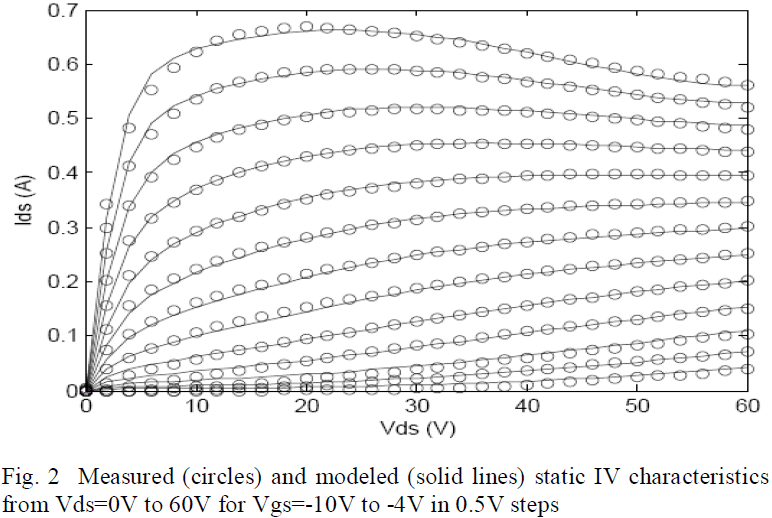
Fig. 2 shows the computed static IV characteristics compared with the measured values for the SiC MESFET for Vgs=-10V to -4V in 0.5V steps, Vds=0V to 60V. The static IV is modeled with 8 polynomial coefficients for an excellent fit. Each data point is measured over a period of a few seconds to allow settling of the current due to dispersive effects. The result is a truly static IV characteristic.
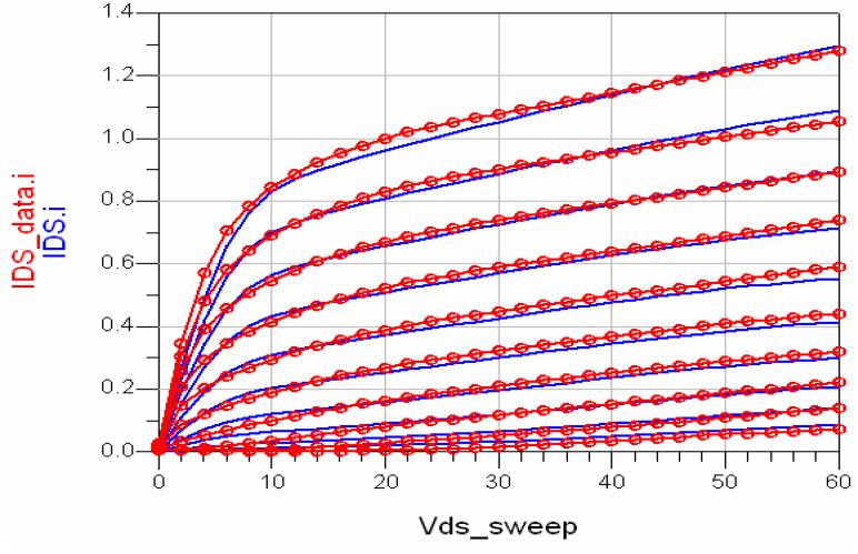
The pulsed IV characteristics of the SiC MESFET biased at Ids=546mA, Vds=48V for a bias range of Vgs=-10V to -1V in 1V steps and Vds=0V to 60V were measured on a Nanometrics DiVA Dynamic I-V Analyzer [10] using 200ns pulses separated by 1ms. The modeled pulsed IV curves compared with the measured data obtained from the final large-signal model are shown in Fig 3.
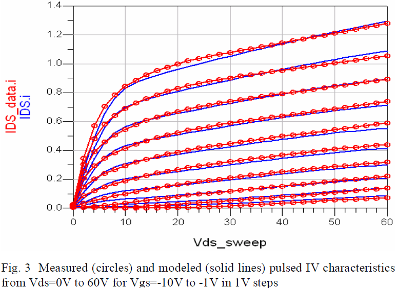
The 200ns pulse width and 1ms pulse period prevent the onset of dispersion during the pulsed state and sufficient relaxation of the dynamic device behavior between pulses [11]. Due to the 30W limit on the measurement system at the time of testing, the PIV data obtained from the device is extrapolated and used for the basis of our large-signal drain current model. Here, Ipk is modeled as a linear function of Vds and Vpk is constant. The tanh(αVds) term is used in modeling the linear regime of the pulsed IV data.
B. Parasitics and Capacitances Modeling
The extrinsic small-signal parameters are extracted based on standard methods [12],[13],[1]. The intrinsic device parameters were extracted from S-parameter measurements taken at Vgs=-10V to -5V in 1V steps for Vds=0V to 60V in 2V steps. The data obtained describing the voltage dependent capacitors Cgs, Cgd and Cds were modeled using the Chalmers capacitance model and implemented into Agilent ADS in the form of charge equations [6],[8]. As a simplification, the same form of capacitance equation is used for all three nonlinear capacitors, allowing a more intuitive initial approximation of the parameters prior to optimization.
C. Diode Modeling
The characteristics of the gate-source and gate-drain diodes in forward conduction are modeled using the standard diode equation. The saturation currents and thermal voltages of the diodes are extracted by measuring the device in forward conduction [14]. These forward conduction gate current measurements are also used to assist in the extraction of the parasitic gate, drain and source resistances as described by Fukui [14].
III. Experimental Model Verification
In this section, the model is compared against measured S-parameter data to verify the small-signal performance and against power data of the output and input reflected harmonics to verify the large-signal accuracy.
A. Small Signal S-Parameters
The S-parameters of the Cree SiC MESFET were measured on an HP 8510B vector network analyzer calibrated using a microstrip TRL calibration from 0.1GHz to 4.0GHz over a range of bias points from Vgs=-10V to -5V in 1V steps for Vds=0V to 60V in 2V steps. The S-parameters of the model compared with measured data at Vgs=-5V and Vds=48V is shown in Fig. 4. According to the plots, the model shows a close agreement to the measured data, verifying the functionality of the model as a small-signal model.
Two drain current sources are often used, one modeling the DC drain current and the other operating at RF frequencies [6] to compensate for differences between gm and gds derived at DC and those derived from S-parameters. The RF current source provides supplementary current such that gm and gds are accurate under RF conditions, but requires additional characterization.
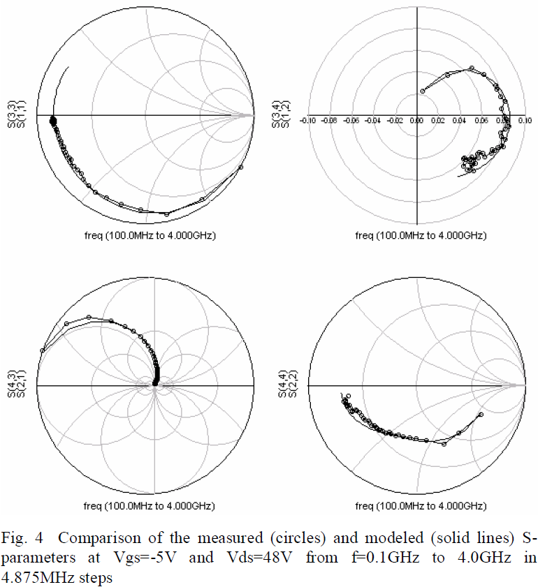
According to the S-parameter data, the single drain current source based on PIV measurements is sufficient in modeling the small-signal gm and gds. With high power devices, it is crucial to consider PIV measurements which do not exhibit the dispersive effects that cause gm and gds derived at dc to be different than those derived at RF.
B. Output and Input Reflected Harmonic Power Generation
The power performance of the model is verified with measured power data. The output and input reflected power of the device at f0=2GHz over an available power range of 10dBm to 36dBm in 1dBm steps is simulated and compared with measured data as shown in Fig. 5 and Fig. 6, respectively.
According to the output power characteristic shown in Figure 5, the model provides a good prediction of the output power for the first three harmonics. At an available source power of +36dBm, the device produces +40dBm, confirming the 10W RF power capability reported in the datasheet [9].
The input reflected power at the first three harmonics also shows good agreement with the measured data as shown in Figure 6. The input reflected power measurements can be used to compute the actual power delivered into the device which may be helpful in understanding and improving the efficiency of high power circuits.
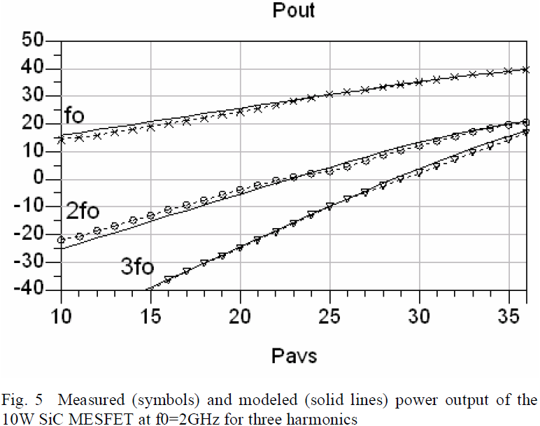
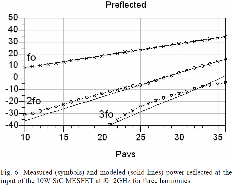
Measuring and characterizing the harmonic power generation at both ports allows a deeper understanding of the device nonlinearities such as the terminal impedances and harmonic generation under large-signal excitation. The power measurements presented here of the unmatched device itself, not of a particular amplifier implementation, which further establishes this as a general device model.
IV. Conclusions
A new large-signal model for SiC MESFET transistors is presented here. A simple, robust drain current model based on the Chalmers model is presented and has demonstrated the ability to model both static and pulsed IV characteristics. The large-signal model has been implemented in ADS and can accurately predict the small-signal S-parameters performance as well as the large-signal output and input reflected power of the device for three harmonics.
Acknowledgment
The authors would like to thank Dr. David McQuate, Dr. Giovonnae Anderson and Dr. Wayne Martin for their generous contributions and support of this work.
References
[1] A. Sayed, “Ultra Wideband 5 W Hybrid Power Amplifier Design Using Silicon Carbide MESFETs,” M.S. Thesis, Technical University of Berlin, Berlin, Germany, 2005.
[2] R.A. Sadler, S.T. Allen, W. L. Pribble, T.S. Alcorn, J.J. Sumakeris and J.W. Palmour, “SiC MESFET hybrid amplifier with 30-W output power at 10 GHz,” IEEE/Cornell Conference on High Performance Devices, 2000. pp. 173 – 177, Aug. 2000.
[3] K. Andersson, V. Desmaris, J. Eriksson, N. Rorsman and H. Zirath, “C-band linear resistive wide bandgap FET mixers,” Microwave Symposium Digest, 2003 IEEE MTT-S International Volume 2. pp. 1303-1306, June 2003.
[4] Z.D. Schwartz, G.E. Ponchak, “1-GHz, 200/spl deg/C, SiC MESFET Clapp oscillator,” IEEE Microwave and Wireless Components Letters, Volume 15, Issue 11. pp. 730-732, Nov. 2005.
[5] I. Angelov, L. Bengtsson, M. Garcia, “Extensions of the Chalmers nonlinear HEMT and MESFET model”, Microwave Theory and Techniques, IEEE Transactions on, vol. 44, pp. 1664 – 1674, Oct. 1996.
[6] I. Angelov, N. Rorsman, J. Stenarson, M. Garcia and H. Zirath, “An Empirical Table-Based FET Model”, IEEE Transactions on Microwave Theory and Techniques, Vol. 47, No. 12, pp. 2350 – 2357, Dec. 1999.
[7] I. Angelov, V. Desmaris, K. Dynefors, P.A. Nilsson, N. Rorsman, H. Zirath, “On the large-signal modeling of AlGaN/GaN HEMTs and SiC MESFETs,” Gallium Arsenide and Other Semiconductor Application Symposium, 2005. EGAAS 2005. pp. 309-312. 3-4 Oct. 2005.
[8] A. Sayed, G. Boeck, “An empirical large signal model for silicon carbide MESFETs,” Gallium Arsenide and Other Semiconductor Application Symposium, 2005. pp. 313-316, Oct. 2005.
[9] Cree, Inc, “CRF24010 10W SiC RF Power MESFET datasheet,” available at http://www.cree.com/products/pdf/CRF24010-Rev1_4.pdf
[10] Nanometrics, “DiVA [Dynamic I-V Analyzer] datasheet,” available at http://www.nanometrics.com/products/Diva.html
[11] P. Ladbrooke, “Pulsed IV Measurement of Semiconductor Devices,” available from Accent, Inc., sales@accentopto.com
[12] G. Dambrine, A. Cappy, F. Heliodore and E. Playez, “A new method for determining the FET small-signal equivalent circuit,” IEEE Transactions on Microwave Theory and Techniques, vol. 36, July 1988, p. 1151-1159.
[13] R. Anholt, Electrical and Thermal Characterization of MESFETs, HEMTs, and HBTs. Boston, Artech House, 1995, pp.36-44.
[14] H. Fukui, “Determinations of the basic parameters of a GaAs MESFET,” Bell Systems Technical Journal, Vol. 58, no. 3, Mar. 1979.