

 0
0
 0
0
By Kelvin Yuk for the completion of EEC218A
Originally published Dec 6, 2001
Abstract
For the project, I propose to do the design and layout of a 4-bit serial adder. The serial adder is composed of two shift registers, one used as an accumulator for the result, a full adder carry flip-clop and a combinational control network. The serial adder adds two numbers together and continues to add the number in the Addend Register to the result in the Accumulator until it is told to stop. The accumulator and addend registers are composed of flip-flops that form a shift register. The full adder and the control circuits are combinational networks. Timing will be measured from the loading of numbers into the registers, shifting of each bit into the full adder and computing the resulting sum. Additional timing considerations can also be measured from the input of the Start signal to the computation of the result.
Design
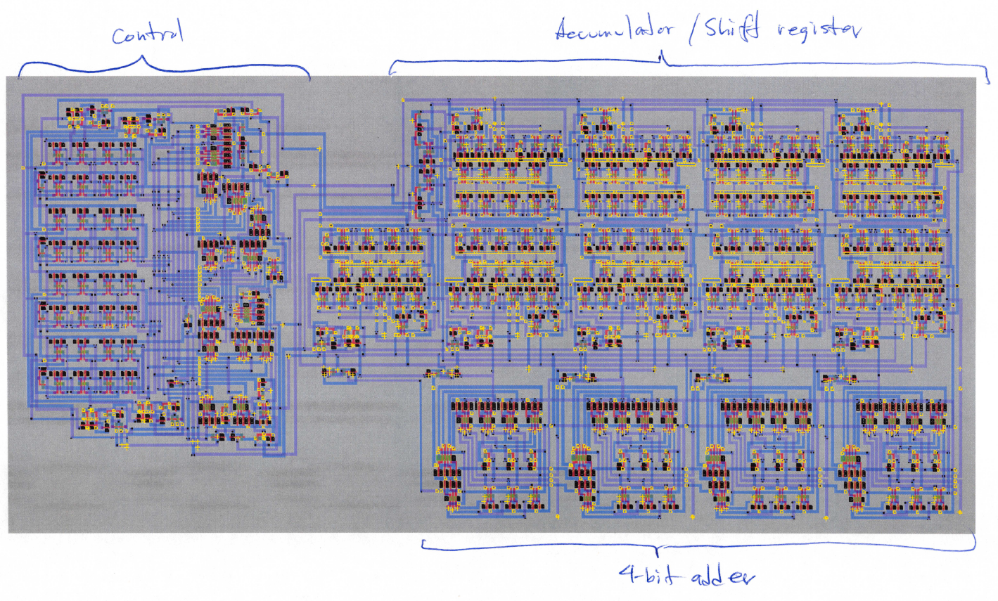
The 4-bit multiplier is composed of three major parts: the control unit, the accumulator/shift register, and the 4-bit adder (Fig 1a).
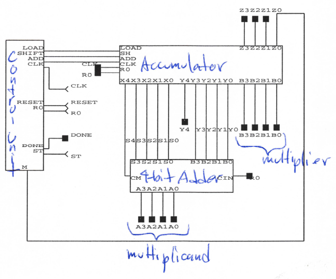
Fig. 1a. Architecture of 4-bit adder
Multiplication is performed by first loading the 4-bit multiplicand into the adder and loading the 4-bit multiplier into the lower 4 flip-flops of the register. The multiplier is shifted out of the register bit-by-bit and checked for a high bit. When the bit is high, the multiplicand is added to the shifted result stored within the register. The control unit sends shift and add signals to the accumulator depending on the value of the bits received from the multiplier. This shifting and adding behavior simulates the shifting and added performed in multiplying two binary numbers by hand.
The control unit is a 10 state Mealy state machine that configures add and shift signals based on the output from the accumulator. The state diagram is shown in Fig 1b. The control unit requires 4 D flip-flops to represent all the states.
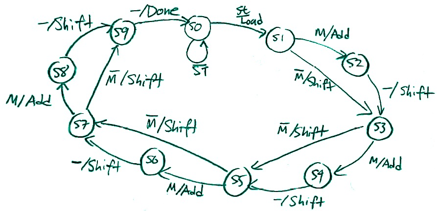
Fig. 1b. Control State Machine
The accumulator/shift registers is composed of 9 modified flip-flops that have load and shift capability. The accumulator is shown in fig 2a. The 4-bit adder is simply a chain of four 1-bit full adders cascaded together fig. 2b
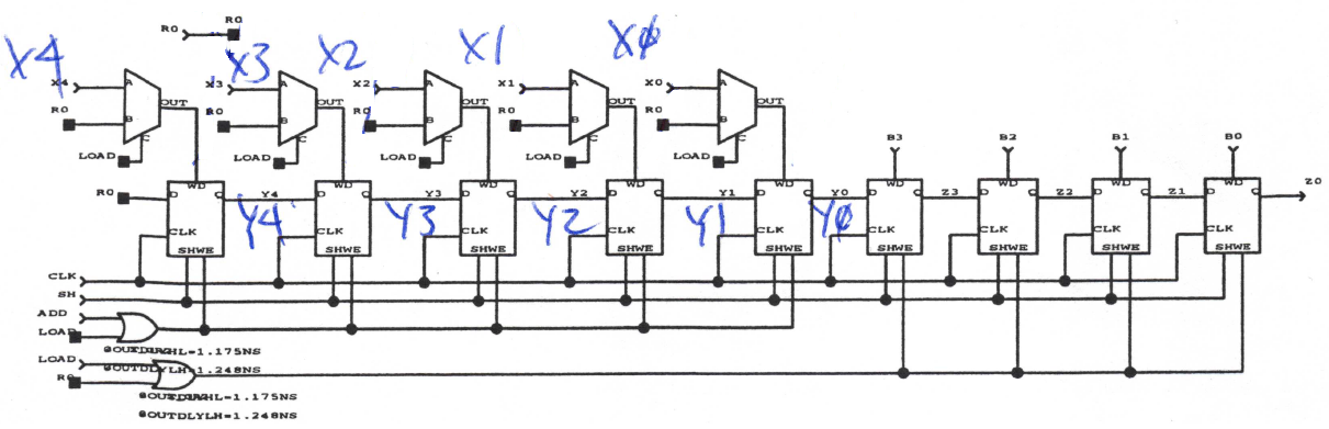
Fig. 2a. Accumulator
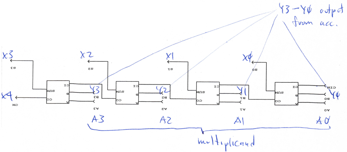
Fig. 2b. 4-bit adder composed of 4 full adders
Layout
The layouts of the basic CMOS gates used for the multiplier are shown in Fig. 3. The unit cells are the inverter and the 2-, 3- and 4-input NAND gates.
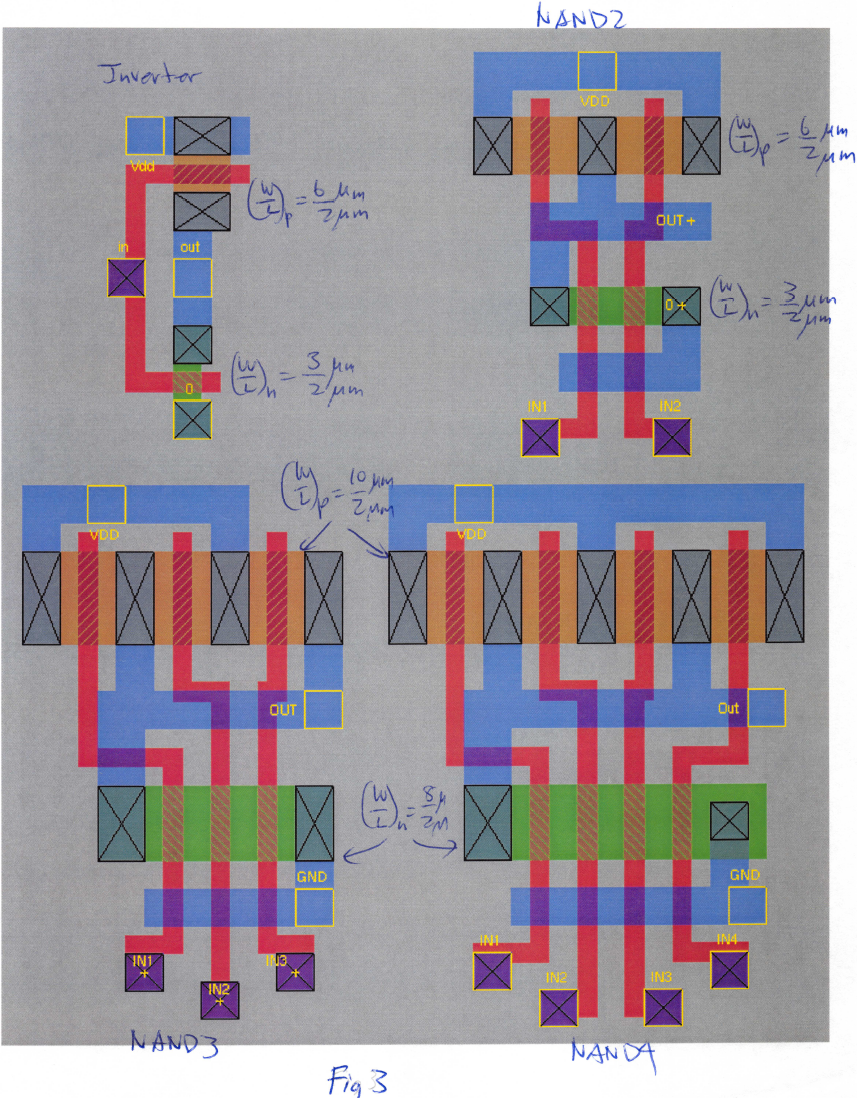
Fig. 3. Layout of basic gates
Inverter
For the inverter, I used a KI=(W/L)n/(W/L)p=(3u/2u)/(6u/2u) because it had the best overall propagation characteristics as learned in previous experiments. For the layout of the cell, I chose to layout gates of the NMOS and the PMOS horizontally instead of vertically in order to save space. This arrangement is more compact for the purposes of my circuit.
2-input NAND, 3-input NAND and 4-input NAND
The layout of the 2-input NAND, 3-input NAND and 4-input NAND is shown in 3. Each NAND gates’ inputs are located at the bottom of the circuit. All NMOS transistors in series share their source with the drain of the NMOS transistor below it and share their drains with the sources above them. Likewise, the PMOS transistors share sources. The output is located in the center of the layout allowing access to the output from both sides of the gate. The NAND2 gate has transistor dimensions
KI = (W/L)N / (W/L)P = (4um/2um) / (6um/2um) . From previous experiments we found that the inversion voltage (VM) and propagation delays depend on the device dimensions and that a KI of around ½ or 1 gave the best overall propagation delays and well-centered VM. Therefore I chose KI = 2/3 which is between KI = ½ and 1. For the NAND3 and NAND4 gate I used KI = (8/2)/(10/2). Although these transistors are wider, the KI ratio is still quite close to 1 and should exhibit good balanced propagation characteristics. I used minimum length because this gives smaller propagation delay.
D Flip-flop w/Shift, Load, Hold
The schematic and interconnect block diagram are shown below. This cell contains a negatively edge-triggered D flip-flop. The gates of the D flip-flop are connected as shown below. The layout of the D shift/load register is shown as a part of the accumulator layout in Fig. 4.
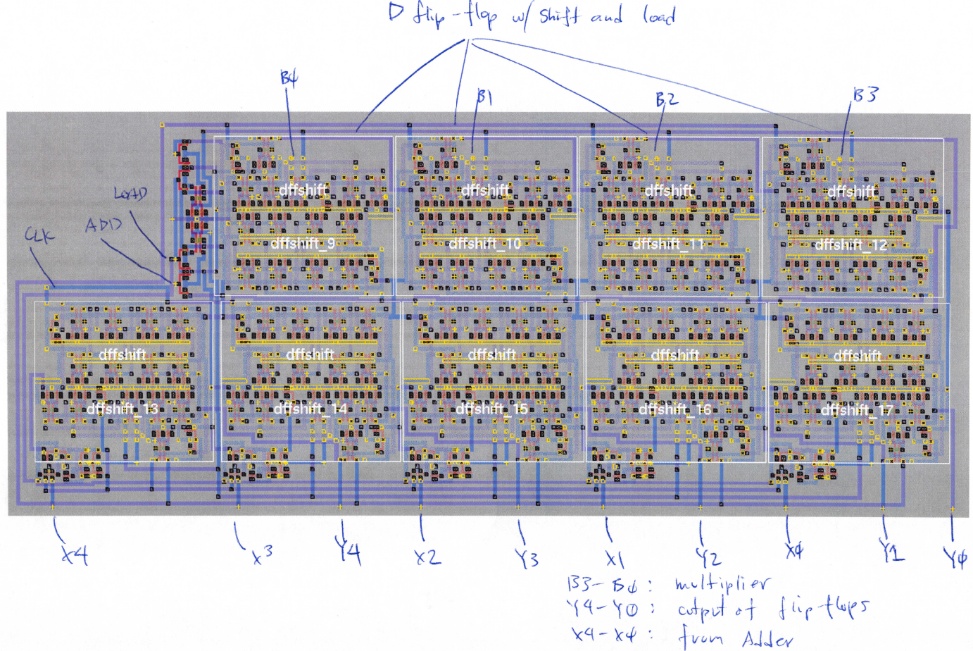
Fig. 4a. Accumulator and shift register
On notable thing about the layout is how the multiplexer and the combinational logic is rotated upside-down in order to fit share power and ground rails and to reduce overall area. Although, the block size or the circuit is not perfect, the gates are more compact using this arrangement.
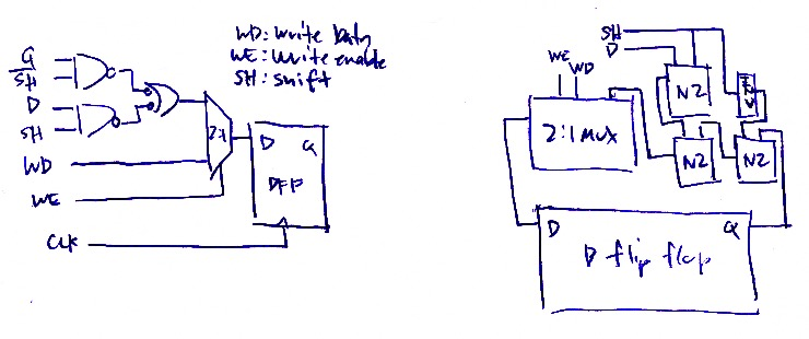
Fig. 4b. D flip-flop with shift, load and hold schematic (left) and interconnect diagram (right)
1-bit Full Adder
The interconnect diagram is shown below. The layout is shown as a part of the 4-bit adder in Fig 5.
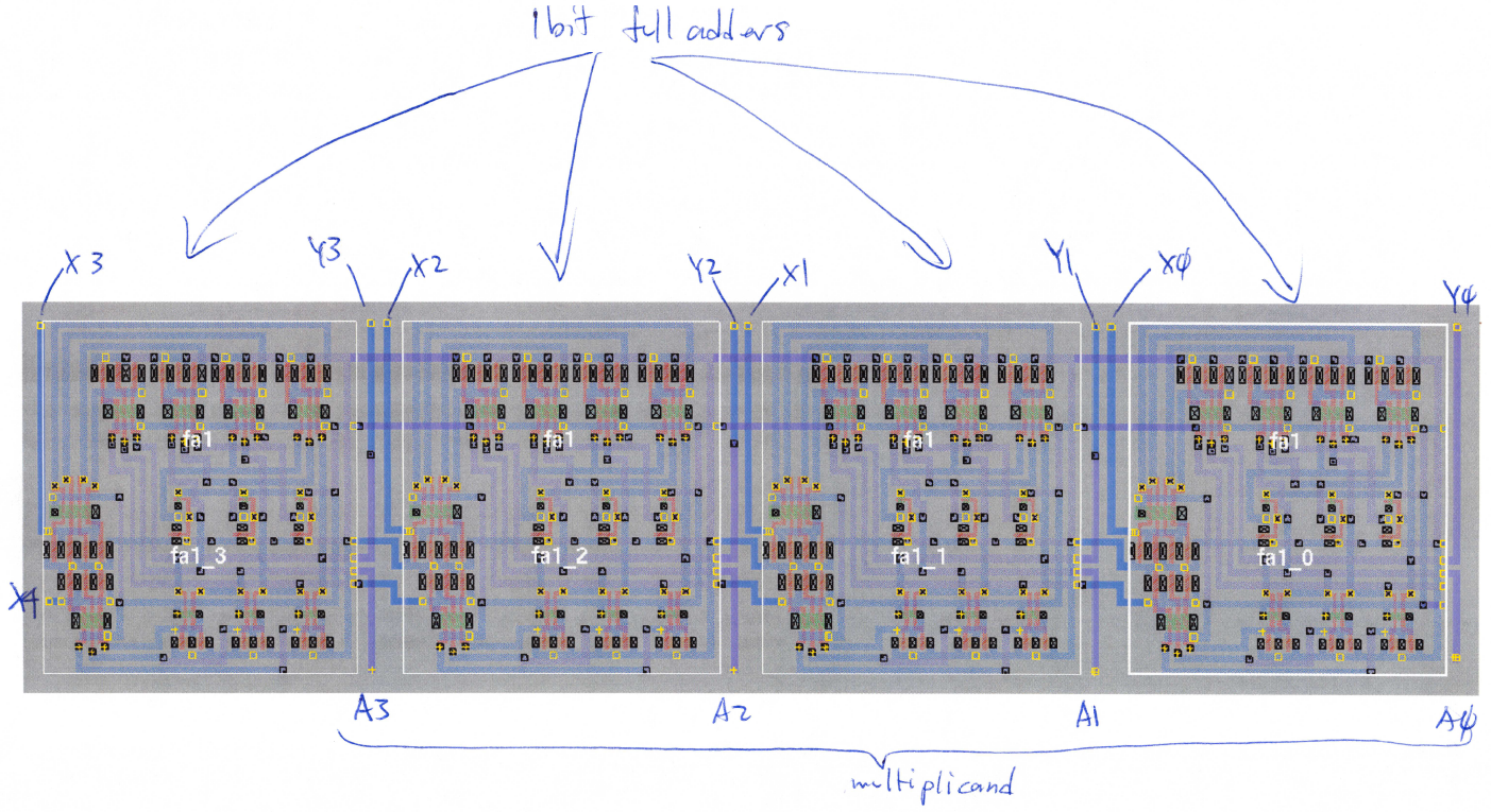
Fig. 5. 4-bit adder
Since there are two outputs of the full adder, Carry Out (Co) and Sum (S), there are essentially two separate functions involved:
Co = AB + ACin + BCin
S = AB’C’ + A’BC’ + A’B’C + ABC
Co and S use the same inputs and so Co is located in the upper portion of the layout and S is in the lower portion of the layout. The inputs are guided through the center of the circuit, between the Co and S logic so that they can be shared between the two functions. Since inverters are only needed for the S function, they too are located in the center row for use by the S logic cells. The cells for the S function are rotated so that the inputs are on top and closer to the adder inputs and inverted adder inputs. Both Co and S outputs are located on the rightmost part of the circuit.
Control
The control unit is shown in Fig 6. It has four D flip-flops and combinational logic to produce the next state and output signals.
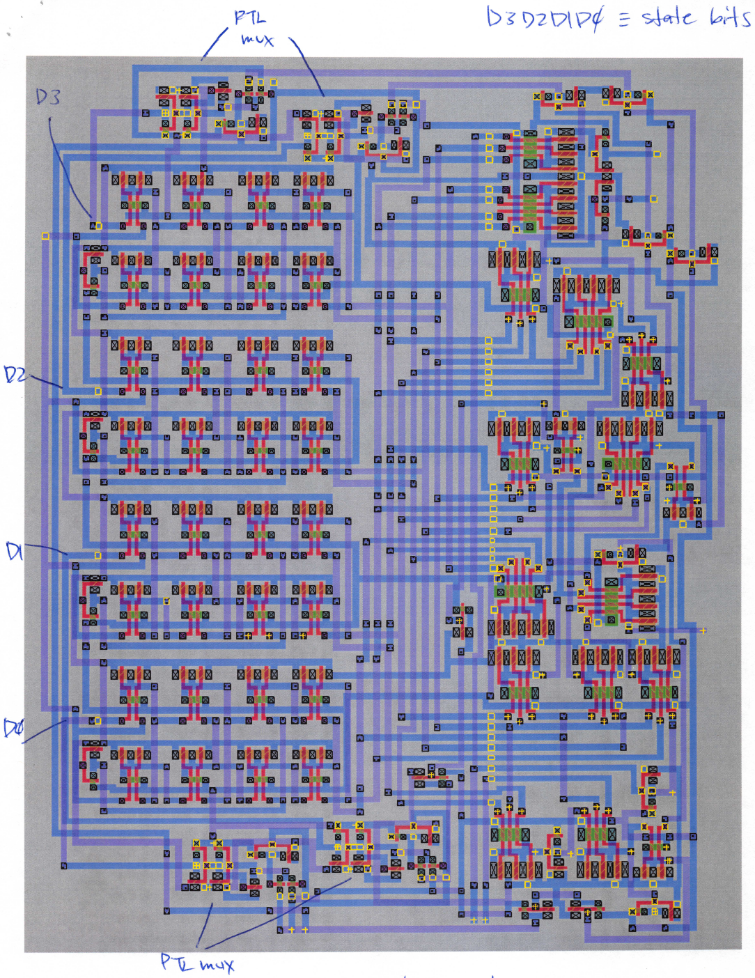
Fig. 6. Control unit
Compact design was the key objective in the laying out the control unit. The D flip-flops are located on the left of the layout and the combinational logic on the right. Passing horizontally through the center is a series of lines that distribute the current state bits to the combinational logic. The combinational logic is arranged in a way to reduce gates by sharing logic outputs and reduce space by rotating and flipping the gates around
Accumulator
The accumulator is composed of nine D shift/load flip-flops cascaded in series. The first five are on the lower portion of the circuit to allow easy access to the 4-bit adder. The last four flip-flops are above the first five in order to reduce the width of the layout. The flip-flops are highlighted in Fig. 4.
4-bit Adder
The layout of the 4-bit adder is shown in Fig. 5. The inputs and outputs of the cell are wired for easy connection to the Accumulator
4-bit Multiplier
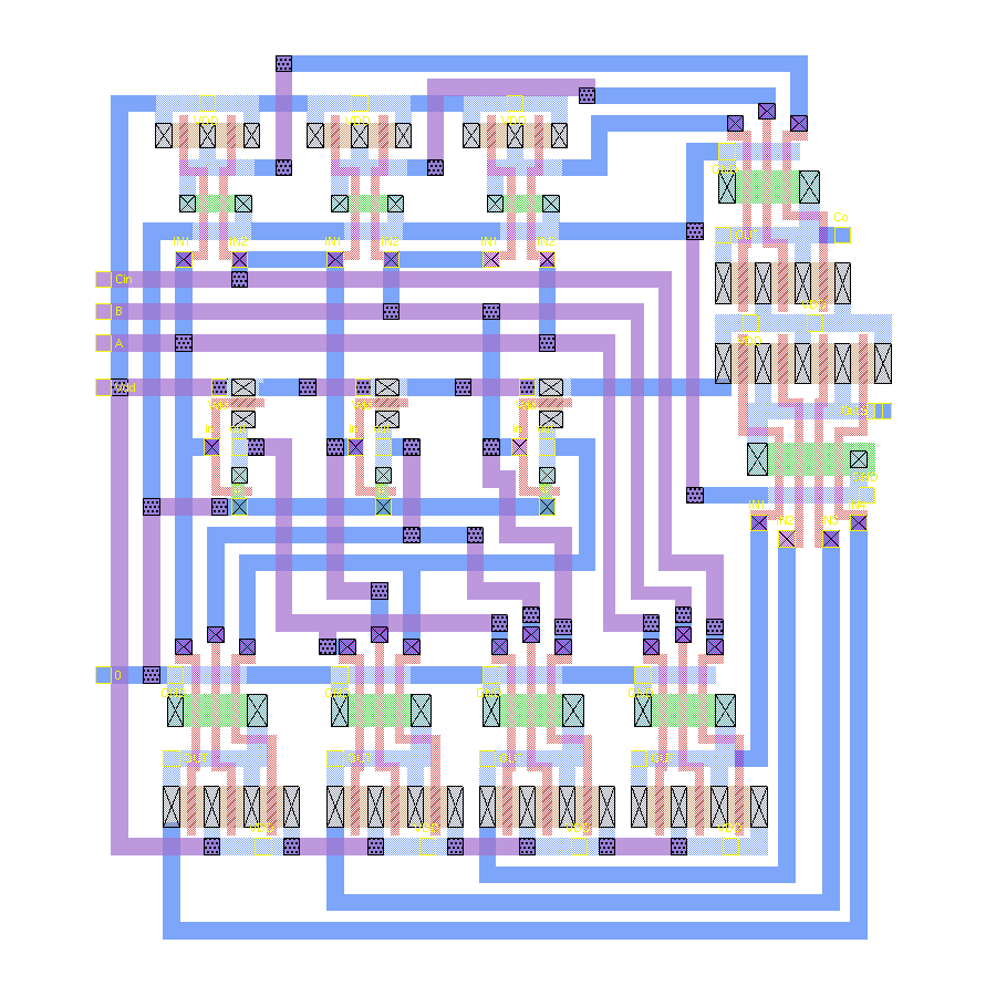
The layout of the 4-bit multiplier is shown in Fig. 7. The three blocks are not optimally connected, however, the empty area is well defined and could be used for other circuits.
Performance verification using SPICE
Propagation delays were measured for each of the basic logic gates. All possible combinations of inputs switching were used to ensure finding the max delay values. The delays were taken over three temperatures T=25, 0 and 70. The waveform for single inputs changes at different temperatures is shown in Fig. 8.
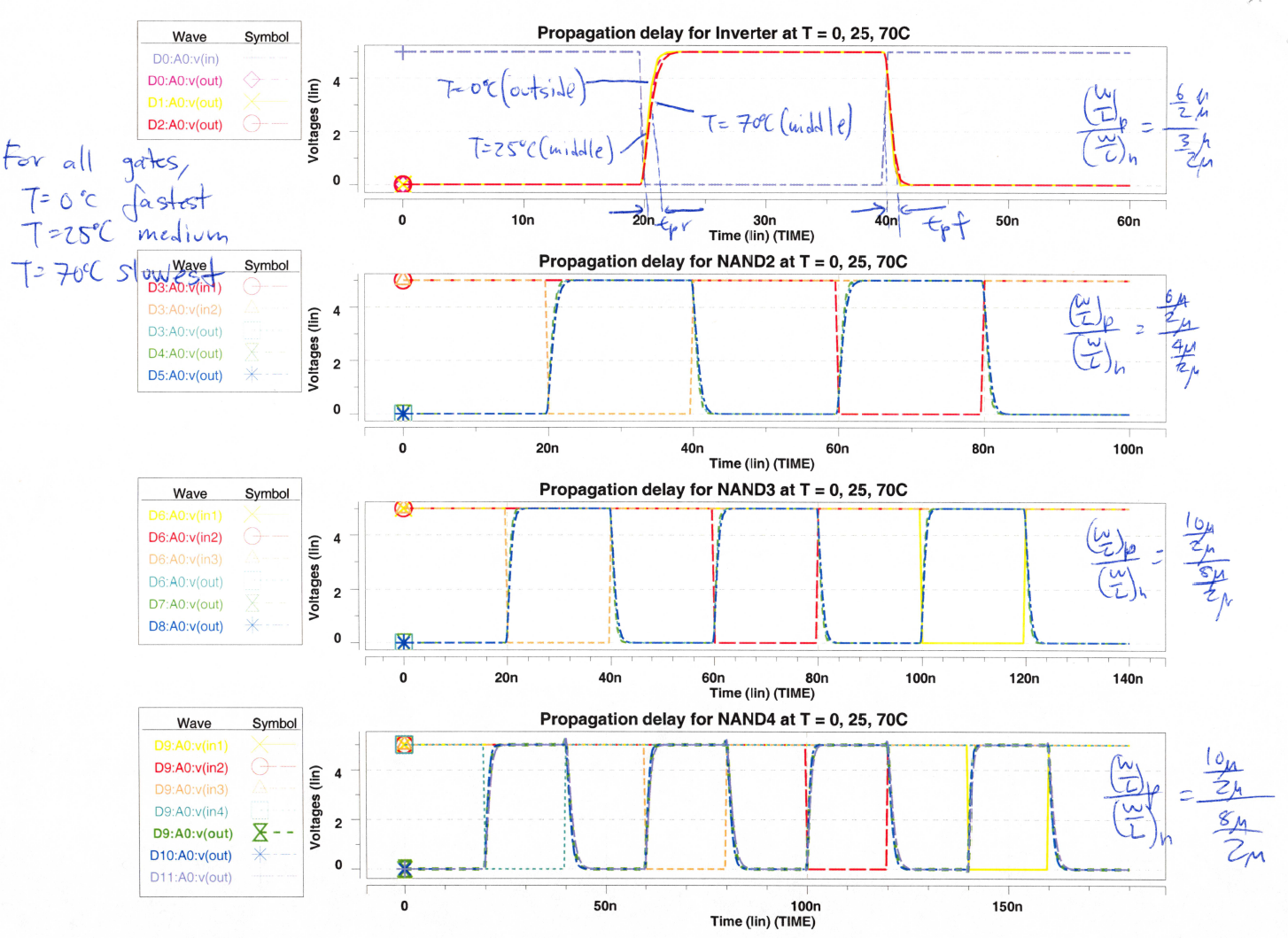
Fig. 8. Timing diagrams to find propagation delays of logic gates
The max propagation delays measured are summarized in the table below with a load of CL=50fF.
Table 1. Max propagation delays of logic gates
| Maximum propagation delays for the 4 logic cells used w/load CL=50fF | |||||||
| Logic cell | Temp (C) | Trise (ns) | Tfall (ns) | Tpr (Out = L->H) | Tpf (Out=H->L) | ||
| Value (ns) | Switching inputs | Value (ns) | Switching inputs | ||||
| INV | 25 | 1.1497 | 0.92206 | 0.58176 | A = H->L | 0.48939 | A=L->H |
| 0 | 1.0731 | 0.84582 | 0.52666 | A = H->L | 0.45590 | A=L->H | |
| 70 | 1.4394 | 1.0256 | 0.68042 | A = H->L | 0.54723 | A=L->H | |
| NAND2 | 25 | 1.3524 | 1.2696 | 0.66575 | B = H->L | 0.68589 | B = L->H |
| 0 | 1.2531 | 1.1739 | 0.60301 | B = H->L | 0.61967 | A, B
= L->H |
|
| 70 | 1.6704 | 1.5118 | 0.77543 | B = H-L> | 0.79548 | B = L->H | |
| NAND3 | 25 | 1.2358 | 1.3350 | 0.63868 | C=H->L | 0.73693 | C= L->H |
| 0 | 1.1553 | 1.1807 | 0.57750 | C=H->L | 0.67227 | B, C
= L->H |
|
| 70 | 1.5626 | 1.5782 | 0.75516 | C=H->L | 0.84245 | C= L->H | |
| NAND4 | 25 | 1.7620 | 2.1754 | 0.89548 | D=H->L | 1.4173 | B, C, D
= L->H |
| 0 | 1.5445 | 1.9346 | 0.79022 | D=H->L | 1.2811 | A,B,C,D = L->H | |
| 70 | 1.9346 | 2.6193 | 1.0874 | D=H->L | 1.6733 | B,C,D
= L->H |
|
The max variation in propagation delay due to temperature is about 0.4ns when dealing with the two extreme values T=0C and T=70C.
VIEWSIM verification of the delay through the critical timing path
The critical path was found by performing simulations in Viewsim with gate delays taken from the layout-extracted SPICE simulations of the basic logic gates. The critical path was found to be between the outputs of the first five accumulator shift flip-flops (Y4 – Y0) through the 4-bit adder and the Write Data muxes and back into the inputs of those same flip-flops. The path is illustrated in Fig. 2. Viewsim simulations were taken at room temperature T=25C so that the critical path could be correctly identified. The delay over the commercial temperature range was simulated in SPICE and is discussed later. The maximum delay that can occur through this path requires specific inputs to carry through the adder and back into the accumulator’s flip-flops. An example of the maximum delay is show below.
Ex. Multiplier: A3A2A1A0 = 1101
Multiplicand: B3B2B1B0 = 1111
Over a period of time, the flip-flops Y4 – Y0 will have 00110. The waveform for this example is shown in fig.
At t–=1.1us (time right before 1.1us) we have at the adder
Carry 1000
Multiplier (A3A2A1A0) 1101
Flip-flop contents (Y4Y3Y2Y1Y0) +(0)0110 Y4 in () is not added
Sum (M4M3M2M1M0) 10011
At t=1.1us, the clock ticks and the contents of registers Y4 – Y0 change to 10011
At t+=1.1us (long after 1.1us)
Carry 1110
Multiplier (A3A2A1A0) 1101
Flip-flop contents (Y4Y3Y2Y1Y0) +(1)0011 Y4 in () is not added
Sum (M4M3M2M1M0) 10000
M3 gives the max delay as seen in Fig. 9. M3 does not stay at 0 as the above implies. It actually changes from 0 => 1 => 0 due to the fact that the carry bits are changing over time. This is seen on the waveform at around t= 1.105us to 1.1078us.
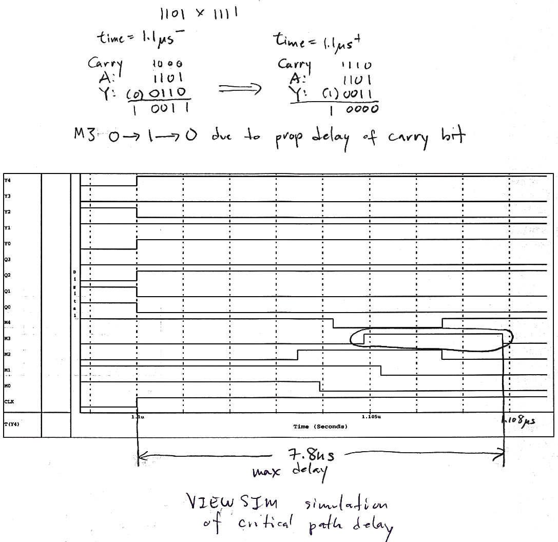
Fig. 9. Critical path delay
Therefore the max delay can be taken from when the outputs of the flip-flops Y4 – Y0 switches to when the write data input M3 reaches a steady state. In VIEWSIM, this delay was 7.8ns
The same max propagation delay measurement was performed on the layout extracted SPICE circuits and at the commercial temperature extremes and room temperature. The waveform for T=25C is shown in Fig. 10. The results from the other temperature are very similar in the plot. At room temperature T=25C, the same propagation delay obtained in VIEWSIM is 16ns. At T=0 and at T=70C, the same propagation delay is about 17ns. This result is interesting because despite the difference in temperature, the max propagation delay remained almost the same. Compared with the VIEWSIM results, though, we can see there is a huge difference in terms of delay. This can be attributed to the capacitance that is added by routing, which is not accounted for in VIEWSIM.
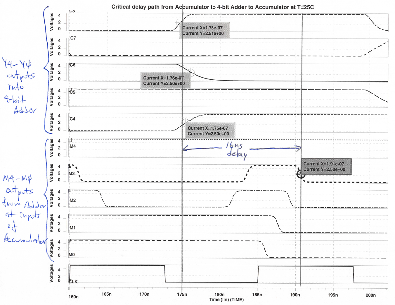
Fig. 10. Critical delay path from accumulator to 4-bit adder to accumulator at T=25C
Total chip power at 20MHz
Power was measured over a complete cycle of operation for the circuit at 20MHz. The power was measured by using SPICE .measure commands for power at the Vdd power supply. Maximum average power was measured by inputting 1111 as both multiplier and the multiplicand. This causes the control to cycle through all of its states and perform the max possible Add and Shift operations. The operation takes approximately 550ns. The average power measured over that time period and is 4.2605mW. Peak power was also measured using SPICE. The transient plot of power is shown in Fig. 11. The power consumption peaks at around 160.1ns at a value of 69.9490mW.
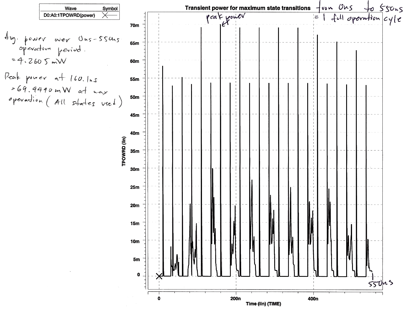
Fig. 11. Transient power for maximum state transitions
Input and output driver
We require that the CMOS circuit to be compatible with TTL circuits and be able to drive a 25pF load. This requires the use of pad drivers. From the TTL load specs given in class:
For output pad driver:
VIHmin = 2.0V; IIHmax = 50uA
VILmax = 0.8V; IILmax = -2mA
For input pad driver:
VOHmax = 2.4V
VOLmax = 0.5V
Output pad driver
The (W/L) ratios required for the PMOS and NMOS transistors of an inverter to meet the output pad driver specs were calculated by driving the output with the respective current and while setting the output to the limiting voltages. The W/L ratio required is given by the drain current equation. From calculations,
(W/L)P = 0.25 for output High
(W/L)N = 13.67 for output Low
The output pad driver is composed of two inverters with different (W/L) ratios.
The output driver has no problem meeting the VOH current and voltage specs since the minimum PMOS size used is well beyond the minimum needed.
In order to meet the VOL requirement, the NMOS transistor needs to be sufficiently sized because it pulls much more current from the TTL during a low output than the PMOS sources to the TTL load during a high output.
The key issue is meeting the 20MHz timing requirement with a 25pF capacitive load. This required even larger PMOS and NMOS transistors. The resulting output pad driver is shown in below
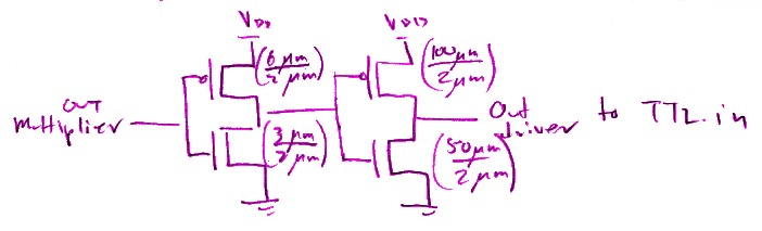 The output pad driver has a tpr of about 12.3ns and a tpf of about 11.4ns as shown in Fig 12 a. This is sufficient to drive the load to the needed voltages before the next clock period. The VOH of the pad driver is 4.98V (fig 12b) and the VOL of the pad driver is 0.4V (fig 12c)
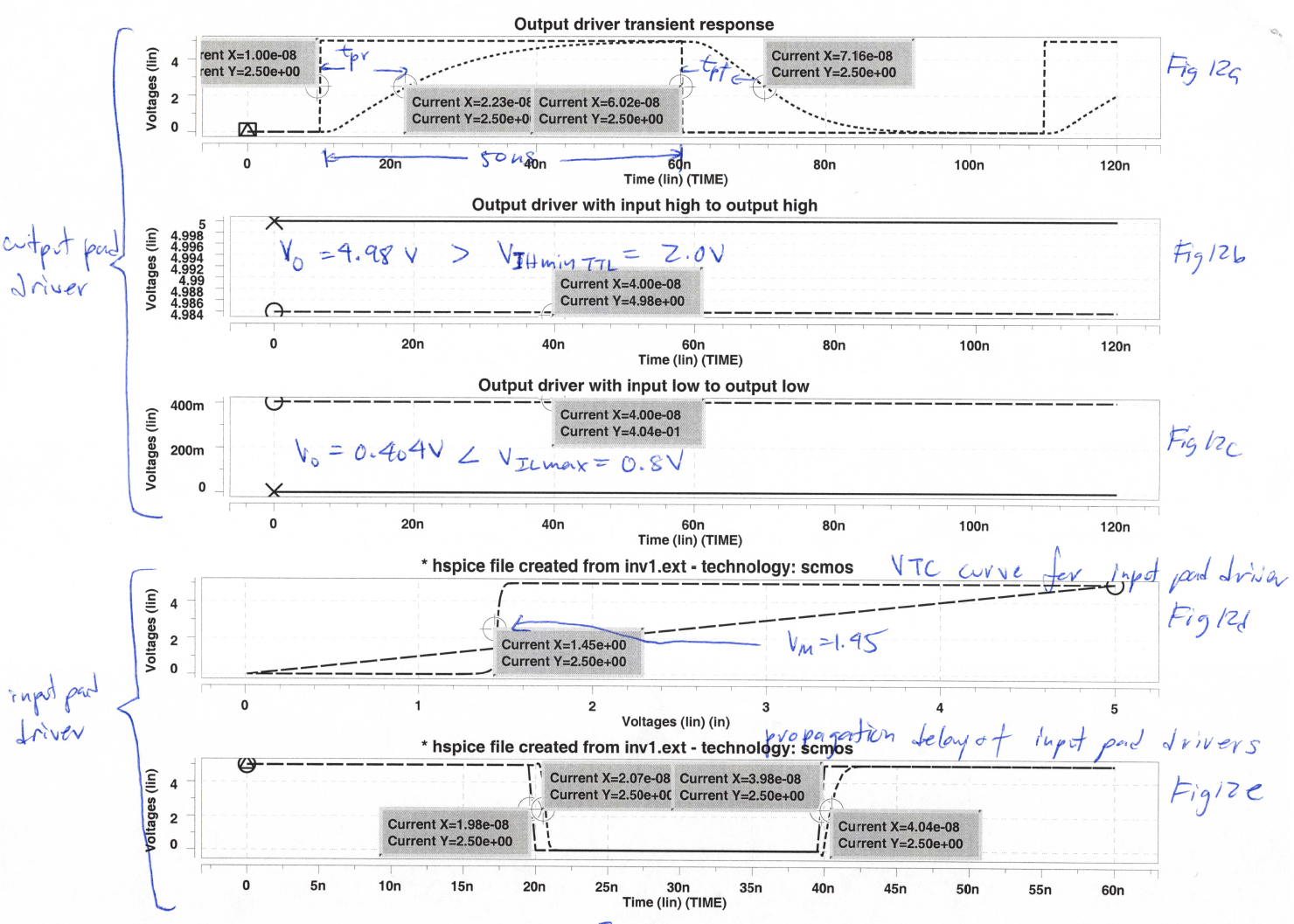
Fig. 12. Output driver transient response
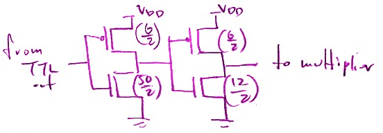
Input pad driver
Since the VOHmin = 2.4 and VOLmax = 0.5V, we need to design the input pad driver to have these voltages as input low and high voltages. To do this we design the inverter of the input pad driver to have an inversion voltage of VM = (2.4+0.5)/2 = 1.45V. The pad driver was built from two inverters, the first being designed to meet the VM requirement. The resulting circuit is shown below
From fig 12d, we see that the inversion voltage is 1.45V and that the propagation delay of the buffer is about tpf = 0.9ns and tpr = 0.6ns (fig. 12e).
Total circuit area of circuit
The total area of the circuit was computed using the MAGIC box command. Because the final layout of the multiplier contains so much open area, I computed the total area by measuring the area of the three major components. The additional routing area can be accounted for in the empty space within the Accumulator box area. The areas of the individual cells and all higher level cells are shown below.
Table 2. Layout area of each cell
| Height (um) | Width (um) | Area (um2) | |
| INV1 | 15 | 34 | 510 |
| NAND2 | 43 | 26 | 1118 |
| NAND3 | 57 | 34 | 1938 |
| NAND4 | 58 | 44 | 2552 |
| DFF | 104 | 192 | 19968 |
| DFFSHIFT | 189 | 214 | 40446 |
| Buffer | 15 | 58 | 870 |
| 2:1 PTL MUX | 49 | 81 | 3969 |
| 2:1 CMOS MUX | 55 | 122 | 6710 |
| 1-bit Full Adder | 221 | 199 | 43979 |
| Accumulator | 456 | 1120 | 510720 |
| Control | 592 | 458 | 271136 |
| 4-bit Adder | 222 | 893 | 198246 |
| Multiplier box | 714 | 1590 | 1135260 |
| Total Area = Area(Accumulator) + Area(Control) + Area(4-bit Adder)
= 510720 um2 + 271136 um2 + 198246 um2 = 980102 um2 = 0.980102 mm2 |
|||
Verification of 20MHz operation
Fig 13 shows the entire waveform for one full operation. The inputs to this example are 1111 (15) x 1111 (15) = 011100001 (225). The clock frequency is 20MHz or clock period T=50ns. The contents of the accumulator is the result at the end of the operation. These outputs are C8 – C0 on the waveform plot.
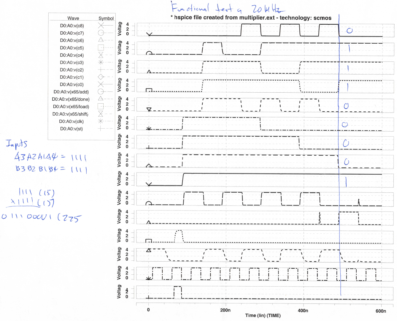
Fig. 13. Functional test at 20 MHz
Development Issues
One of the major problems sources I encountered involves the 2:1 PTL multiplexer. I designed the multiplexer to save on the number of transistors needed to realize the switching action. However, the PTL transistors gave me problems with driving the multiplexer. On more than one occasion, I had voltages around 1V at the inputs of the PTL mux that should have been 0 from the output of the driving CMOS gate. I speculate that the problem is due to the effect that routing and parasitic capacitances have on the lines driving the PTL source. To alleviate this problem, I had to insert CMOS buffers composed of two inverters to drive the appropriate logic swing.
Conclusion
This IC design project has demonstrated the complexity of a custom-designed circuit. Loading, timing, power and compatibility with other logic families are a few of the major considerations to be evaluated when designing a circuit. I had problems with PTL that resulted in additional debug and development time. Some things that could have been improved upon are finding a simpler implementation of the multiply function. Reducing routing capacitance can be a challenge and so generates much more propagation delay that would normally be expected from a high level simulation.